

564
Y. Wang et al.
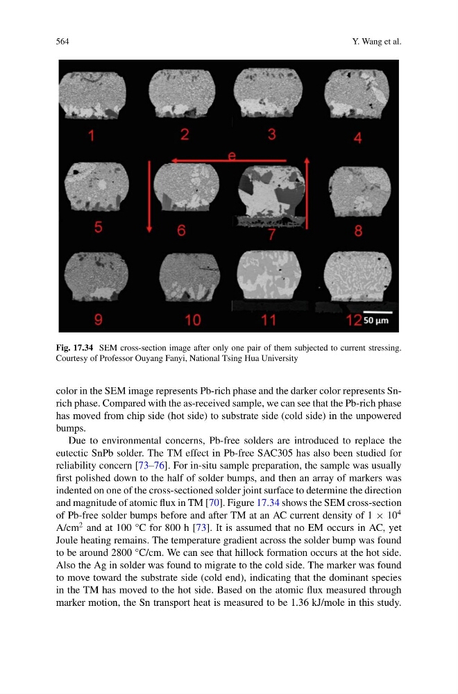
Fig. 17.34 SEM cross-section image after only one pair of them subjected to current stressing.
Courtesy of Professor Ouyang Fanyi, National Tsing Hua University
color in the SEM image represents Pb-rich phase and the darker color represents Snrich phase. Compared with the as-received sample, we can see that the Pb-rich phase
has moved from chip side (hot side) to substrate side (cold side) in the unpowered
bumps.
Due to environmental concerns, Pb-free solders are introduced to replace the
eutectic SnPb solder. The TM effect in Pb-free SAC305 has also been studied for
reliability concern [73–76]. For in-situ sample preparation, the sample was usually
first polished down to the half of solder bumps, and then an array of markers was
indented on one of the cross-sectioned solder joint surface to determine the direction
and magnitude of atomic flux in TM [70]. Figure 17.34 shows the SEM cross-section
of Pb-free solder bumps before and after TM at an AC current density of 1 × 10
4
A/cm
2 and at 100 °C for 800 h [73]. It is assumed that no EM occurs in AC, yet
Joule heating remains. The temperature gradient across the solder bump was found
to be around 2800 °C/cm. We can see that hillock formation occurs at the hot side.
Also the Ag in solder was found to migrate to the cold side. The marker was found
to move toward the substrate side (cold end), indicating that the dominant species
in the TM has moved to the hot side. Based on the atomic flux measured through
marker motion, the Sn transport heat is measured to be 1.36 kJ/mole in this study.
Y. Wang et al.
Fig. 17.34 SEM cross-section image after only one pair of them subjected to current stressing.
Courtesy of Professor Ouyang Fanyi, National Tsing Hua University
color in the SEM image represents Pb-rich phase and the darker color represents Snrich phase. Compared with the as-received sample, we can see that the Pb-rich phase
has moved from chip side (hot side) to substrate side (cold side) in the unpowered
bumps.
Due to environmental concerns, Pb-free solders are introduced to replace the
eutectic SnPb solder. The TM effect in Pb-free SAC305 has also been studied for
reliability concern [73–76]. For in-situ sample preparation, the sample was usually
first polished down to the half of solder bumps, and then an array of markers was
indented on one of the cross-sectioned solder joint surface to determine the direction
and magnitude of atomic flux in TM [70]. Figure 17.34 shows the SEM cross-section
of Pb-free solder bumps before and after TM at an AC current density of 1 × 10
4
A/cm
2 and at 100 °C for 800 h [73]. It is assumed that no EM occurs in AC, yet
Joule heating remains. The temperature gradient across the solder bump was found
to be around 2800 °C/cm. We can see that hillock formation occurs at the hot side.
Also the Ag in solder was found to migrate to the cold side. The marker was found
to move toward the substrate side (cold end), indicating that the dominant species
in the TM has moved to the hot side. Based on the atomic flux measured through
marker motion, the Sn transport heat is measured to be 1.36 kJ/mole in this study.