

17 Interconnect Quality and Reliability of 3D Packaging
563
17.6.2 Fundamentals of Thermomigration
TM is the phenomenon of atomic diffusion driven by a temperature gradient. Classically, it is called the Soret effect. Mathematically, the driving force of TM can be
expressed as
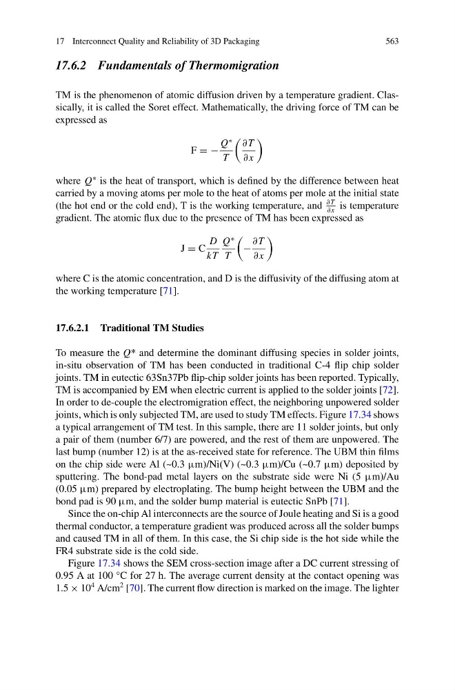
F = −
Q
∗
T
∂ T
∂ x
where Q
∗ is the heat of transport, which is defined by the difference between heat
carried by a moving atoms per mole to the heat of atoms per mole at the initial state
(the hot end or the cold end), T is the working temperature, and
∂ T
∂ x
is temperature
gradient. The atomic flux due to the presence of TM has been expressed as
J = C
D
kT
Q
∗
T
−
∂ T
∂ x
where C is the atomic concentration, and D is the diffusivity of the diffusing atom at
the working temperature [71].
17.6.2.1 Traditional TM Studies
To measure the Q* and determine the dominant diffusing species in solder joints,
in-situ observation of TM has been conducted in traditional C-4 flip chip solder
joints. TM in eutectic 63Sn37Pb flip-chip solder joints has been reported. Typically,
TM is accompanied by EM when electric current is applied to the solder joints [72].
In order to de-couple the electromigration effect, the neighboring unpowered solder
joints, which is only subjected TM, are used to study TM effects. Figure 17.34 shows
a typical arrangement of TM test. In this sample, there are 11 solder joints, but only
a pair of them (number 6/7) are powered, and the rest of them are unpowered. The
last bump (number 12) is at the as-received state for reference. The UBM thin films
on the chip side were Al (~0.3 μm)/Ni(V) (~0.3 μm)/Cu (~0.7 μm) deposited by
sputtering. The bond-pad metal layers on the substrate side were Ni (5 μm)/Au
(0.05 μm) prepared by electroplating. The bump height between the UBM and the
bond pad is 90 μm, and the solder bump material is eutectic SnPb [71].
Since the on-chip Al interconnects are the source of Joule heating and Si is a good
thermal conductor, a temperature gradient was produced across all the solder bumps
and caused TM in all of them. In this case, the Si chip side is the hot side while the
FR4 substrate side is the cold side.
Figure 17.34 shows the SEM cross-section image after a DC current stressing of
0.95 A at 100 °C for 27 h. The average current density at the contact opening was
1.5 × 10
4 A/cm
2 [70]. The current flow direction is marked on the image. The lighter
563
17.6.2 Fundamentals of Thermomigration
TM is the phenomenon of atomic diffusion driven by a temperature gradient. Classically, it is called the Soret effect. Mathematically, the driving force of TM can be
expressed as
F = −
Q
∗
T
∂ T
∂ x
where Q
∗ is the heat of transport, which is defined by the difference between heat
carried by a moving atoms per mole to the heat of atoms per mole at the initial state
(the hot end or the cold end), T is the working temperature, and
∂ T
∂ x
is temperature
gradient. The atomic flux due to the presence of TM has been expressed as
J = C
D
kT
Q
∗
T
−
∂ T
∂ x
where C is the atomic concentration, and D is the diffusivity of the diffusing atom at
the working temperature [71].
17.6.2.1 Traditional TM Studies
To measure the Q* and determine the dominant diffusing species in solder joints,
in-situ observation of TM has been conducted in traditional C-4 flip chip solder
joints. TM in eutectic 63Sn37Pb flip-chip solder joints has been reported. Typically,
TM is accompanied by EM when electric current is applied to the solder joints [72].
In order to de-couple the electromigration effect, the neighboring unpowered solder
joints, which is only subjected TM, are used to study TM effects. Figure 17.34 shows
a typical arrangement of TM test. In this sample, there are 11 solder joints, but only
a pair of them (number 6/7) are powered, and the rest of them are unpowered. The
last bump (number 12) is at the as-received state for reference. The UBM thin films
on the chip side were Al (~0.3 μm)/Ni(V) (~0.3 μm)/Cu (~0.7 μm) deposited by
sputtering. The bond-pad metal layers on the substrate side were Ni (5 μm)/Au
(0.05 μm) prepared by electroplating. The bump height between the UBM and the
bond pad is 90 μm, and the solder bump material is eutectic SnPb [71].
Since the on-chip Al interconnects are the source of Joule heating and Si is a good
thermal conductor, a temperature gradient was produced across all the solder bumps
and caused TM in all of them. In this case, the Si chip side is the hot side while the
FR4 substrate side is the cold side.
Figure 17.34 shows the SEM cross-section image after a DC current stressing of
0.95 A at 100 °C for 27 h. The average current density at the contact opening was
1.5 × 10
4 A/cm
2 [70]. The current flow direction is marked on the image. The lighter