

2 3D Packaging Architectures and Assembly Process Design
39
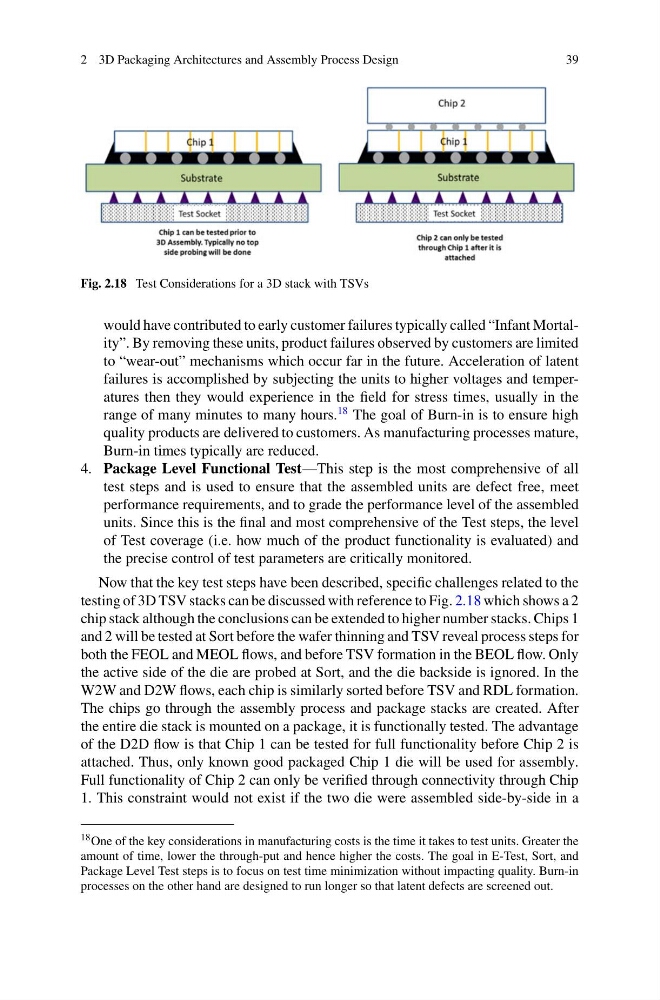
Fig. 2.18 Test Considerations for a 3D stack with TSVs
would have contributed to early customer failures typically called “Infant Mortality”. By removing these units, product failures observed by customers are limited
to “wear-out” mechanisms which occur far in the future. Acceleration of latent
failures is accomplished by subjecting the units to higher voltages and temperatures then they would experience in the field for stress times, usually in the
range of many minutes to many hours.
18 The goal of Burn-in is to ensure high
quality products are delivered to customers. As manufacturing processes mature,
Burn-in times typically are reduced.
4. Package Level Functional Test—This step is the most comprehensive of all
test steps and is used to ensure that the assembled units are defect free, meet
performance requirements, and to grade the performance level of the assembled
units. Since this is the final and most comprehensive of the Test steps, the level
of Test coverage (i.e. how much of the product functionality is evaluated) and
the precise control of test parameters are critically monitored.
Now that the key test steps have been described, specific challenges related to the
testing of 3D TSV stacks can be discussed with reference to Fig. 2.18 which shows a 2
chip stack although the conclusions can be extended to higher number stacks. Chips 1
and 2 will be tested at Sort before the wafer thinning and TSV reveal process steps for
both the FEOL and MEOL flows, and before TSV formation in the BEOL flow. Only
the active side of the die are probed at Sort, and the die backside is ignored. In the
W2W and D2W flows, each chip is similarly sorted before TSV and RDL formation.
The chips go through the assembly process and package stacks are created. After
the entire die stack is mounted on a package, it is functionally tested. The advantage
of the D2D flow is that Chip 1 can be tested for full functionality before Chip 2 is
attached. Thus, only known good packaged Chip 1 die will be used for assembly.
Full functionality of Chip 2 can only be verified through connectivity through Chip
1. This constraint would not exist if the two die were assembled side-by-side in a
18 One of the key considerations in manufacturing costs is the time it takes to test units. Greater the
amount of time, lower the through-put and hence higher the costs. The goal in E-Test, Sort, and
Package Level Test steps is to focus on test time minimization without impacting quality. Burn-in
processes on the other hand are designed to run longer so that latent defects are screened out.
39
Fig. 2.18 Test Considerations for a 3D stack with TSVs
would have contributed to early customer failures typically called “Infant Mortality”. By removing these units, product failures observed by customers are limited
to “wear-out” mechanisms which occur far in the future. Acceleration of latent
failures is accomplished by subjecting the units to higher voltages and temperatures then they would experience in the field for stress times, usually in the
range of many minutes to many hours.
18 The goal of Burn-in is to ensure high
quality products are delivered to customers. As manufacturing processes mature,
Burn-in times typically are reduced.
4. Package Level Functional Test—This step is the most comprehensive of all
test steps and is used to ensure that the assembled units are defect free, meet
performance requirements, and to grade the performance level of the assembled
units. Since this is the final and most comprehensive of the Test steps, the level
of Test coverage (i.e. how much of the product functionality is evaluated) and
the precise control of test parameters are critically monitored.
Now that the key test steps have been described, specific challenges related to the
testing of 3D TSV stacks can be discussed with reference to Fig. 2.18 which shows a 2
chip stack although the conclusions can be extended to higher number stacks. Chips 1
and 2 will be tested at Sort before the wafer thinning and TSV reveal process steps for
both the FEOL and MEOL flows, and before TSV formation in the BEOL flow. Only
the active side of the die are probed at Sort, and the die backside is ignored. In the
W2W and D2W flows, each chip is similarly sorted before TSV and RDL formation.
The chips go through the assembly process and package stacks are created. After
the entire die stack is mounted on a package, it is functionally tested. The advantage
of the D2D flow is that Chip 1 can be tested for full functionality before Chip 2 is
attached. Thus, only known good packaged Chip 1 die will be used for assembly.
Full functionality of Chip 2 can only be verified through connectivity through Chip
1. This constraint would not exist if the two die were assembled side-by-side in a
18 One of the key considerations in manufacturing costs is the time it takes to test units. Greater the
amount of time, lower the through-put and hence higher the costs. The goal in E-Test, Sort, and
Package Level Test steps is to focus on test time minimization without impacting quality. Burn-in
processes on the other hand are designed to run longer so that latent defects are screened out.