

38
R. Mahajan and B. Sankman
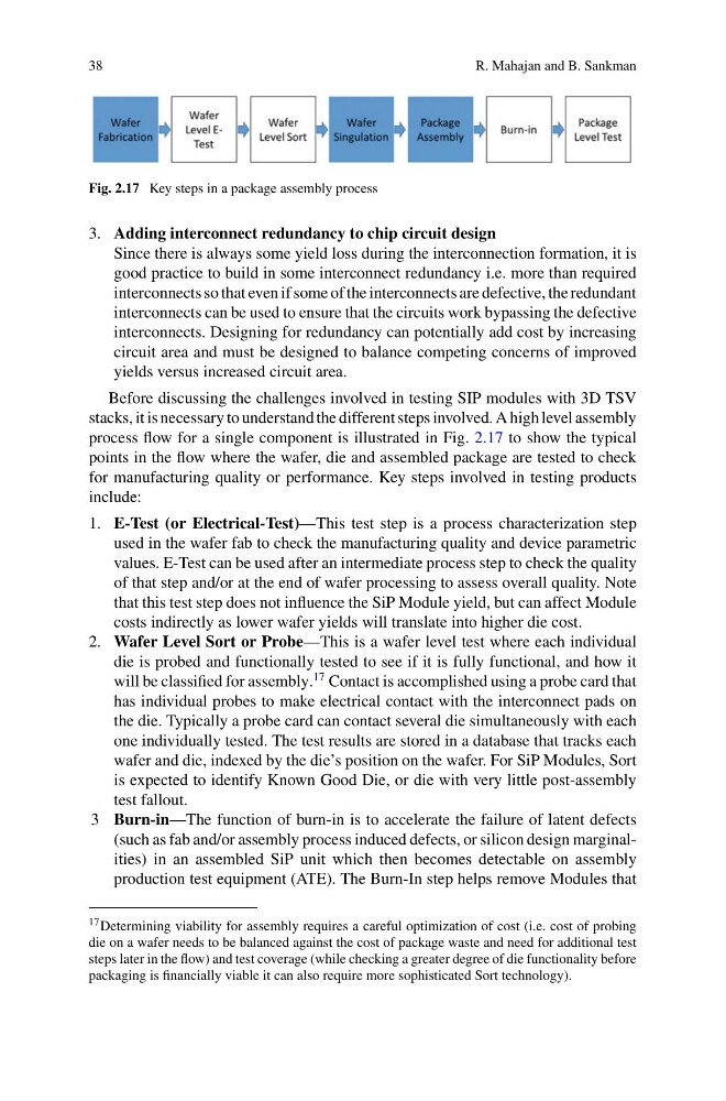
Fig. 2.17 Key steps in a package assembly process
3. Adding interconnect redundancy to chip circuit design
Since there is always some yield loss during the interconnection formation, it is
good practice to build in some interconnect redundancy i.e. more than required
interconnects so that even if some of the interconnects are defective, the redundant
interconnects can be used to ensure that the circuits work bypassing the defective
interconnects. Designing for redundancy can potentially add cost by increasing
circuit area and must be designed to balance competing concerns of improved
yields versus increased circuit area.
Before discussing the challenges involved in testing SIP modules with 3D TSV
stacks, it is necessary to understand the different steps involved. A high level assembly
process flow for a single component is illustrated in Fig. 2.17 to show the typical
points in the flow where the wafer, die and assembled package are tested to check
for manufacturing quality or performance. Key steps involved in testing products
include:
1. E-Test (or Electrical-Test)—This test step is a process characterization step
used in the wafer fab to check the manufacturing quality and device parametric
values. E-Test can be used after an intermediate process step to check the quality
of that step and/or at the end of wafer processing to assess overall quality. Note
that this test step does not influence the SiP Module yield, but can affect Module
costs indirectly as lower wafer yields will translate into higher die cost.
2. Wafer Level Sort or Probe—This is a wafer level test where each individual
die is probed and functionally tested to see if it is fully functional, and how it
will be classified for assembly.
17 Contact is accomplished using a probe card that
has individual probes to make electrical contact with the interconnect pads on
the die. Typically a probe card can contact several die simultaneously with each
one individually tested. The test results are stored in a database that tracks each
wafer and die, indexed by the die’s position on the wafer. For SiP Modules, Sort
is expected to identify Known Good Die, or die with very little post-assembly
test fallout.
3 Burn-in—The function of burn-in is to accelerate the failure of latent defects
(such as fab and/or assembly process induced defects, or silicon design marginalities) in an assembled SiP unit which then becomes detectable on assembly
production test equipment (ATE). The Burn-In step helps remove Modules that
17 Determining viability for assembly requires a careful optimization of cost (i.e. cost of probing
die on a wafer needs to be balanced against the cost of package waste and need for additional test
steps later in the flow) and test coverage (while checking a greater degree of die functionality before
packaging is financially viable it can also require more sophisticated Sort technology).
R. Mahajan and B. Sankman
Fig. 2.17 Key steps in a package assembly process
3. Adding interconnect redundancy to chip circuit design
Since there is always some yield loss during the interconnection formation, it is
good practice to build in some interconnect redundancy i.e. more than required
interconnects so that even if some of the interconnects are defective, the redundant
interconnects can be used to ensure that the circuits work bypassing the defective
interconnects. Designing for redundancy can potentially add cost by increasing
circuit area and must be designed to balance competing concerns of improved
yields versus increased circuit area.
Before discussing the challenges involved in testing SIP modules with 3D TSV
stacks, it is necessary to understand the different steps involved. A high level assembly
process flow for a single component is illustrated in Fig. 2.17 to show the typical
points in the flow where the wafer, die and assembled package are tested to check
for manufacturing quality or performance. Key steps involved in testing products
include:
1. E-Test (or Electrical-Test)—This test step is a process characterization step
used in the wafer fab to check the manufacturing quality and device parametric
values. E-Test can be used after an intermediate process step to check the quality
of that step and/or at the end of wafer processing to assess overall quality. Note
that this test step does not influence the SiP Module yield, but can affect Module
costs indirectly as lower wafer yields will translate into higher die cost.
2. Wafer Level Sort or Probe—This is a wafer level test where each individual
die is probed and functionally tested to see if it is fully functional, and how it
will be classified for assembly.
17 Contact is accomplished using a probe card that
has individual probes to make electrical contact with the interconnect pads on
the die. Typically a probe card can contact several die simultaneously with each
one individually tested. The test results are stored in a database that tracks each
wafer and die, indexed by the die’s position on the wafer. For SiP Modules, Sort
is expected to identify Known Good Die, or die with very little post-assembly
test fallout.
3 Burn-in—The function of burn-in is to accelerate the failure of latent defects
(such as fab and/or assembly process induced defects, or silicon design marginalities) in an assembled SiP unit which then becomes detectable on assembly
production test equipment (ATE). The Burn-In step helps remove Modules that
17 Determining viability for assembly requires a careful optimization of cost (i.e. cost of probing
die on a wafer needs to be balanced against the cost of package waste and need for additional test
steps later in the flow) and test coverage (while checking a greater degree of die functionality before
packaging is financially viable it can also require more sophisticated Sort technology).