

17 Interconnect Quality and Reliability of 3D Packaging
557
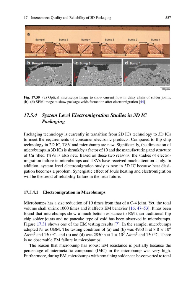
Fig. 17.30 (a) Optical microscope image to show current flow in daisy chain of solder joints.
(b)–(d) SEM image to show package voids formation after electromigration [44]
17.5.4 System Level Electromigration Studies in 3D IC
Packaging
Packaging technology is currently in transition from 2D ICs technology to 3D ICs
to meet the requirements of consumer electronic products. Compared to flip chip
technology in 2D IC, TSV and microbump are new. Significantly, the dimension of
microbumps in 3D ICs is shrunk by a factor of 10 and the manufacturing and structure
of Cu filled TSVs is also new. Based on these two reasons, the studies of electromigration failure in microbumps and TSVs have received much attention lately. In
addition, system level electromigration study is new in 3D IC because heat dissipation becomes a problem. Synergistic effect of Joule heating and electromigration
will be the trend of reliability failure in the near future.
17.5.4.1 Electromigration in Microbumps
Microbumps has a size reduction of 10 times from that of a C-4 joint. Yet, the total
volume shall shrink 1000 times and it affects EM behavior [16, 47–53]. It has been
found that microbumps show a much better resistance to EM than traditional flip
chip solder joints and no pancake type of void has been observed in microbumps.
Figure 17.31 shows one of the EM testing results [7]. In the sample, microbumps
adopted Ni as UBM. The testing condition of (a) and (b) was 4950 h at 8 8 × 10
4
A/cm
2 and 150 °C, and (c) and (d) was 2850 h at 1 × 10
5 A/cm
2 and 150 °C. There
is no observable EM failure in microbumps.
The reason that microbump has robust EM resistance is partially because the
percentage of intermetallic compound (IMC) in the microbump was very high.
Furthermore, during EM, microbumps with remaining solder can be converted to total
557
Fig. 17.30 (a) Optical microscope image to show current flow in daisy chain of solder joints.
(b)–(d) SEM image to show package voids formation after electromigration [44]
17.5.4 System Level Electromigration Studies in 3D IC
Packaging
Packaging technology is currently in transition from 2D ICs technology to 3D ICs
to meet the requirements of consumer electronic products. Compared to flip chip
technology in 2D IC, TSV and microbump are new. Significantly, the dimension of
microbumps in 3D ICs is shrunk by a factor of 10 and the manufacturing and structure
of Cu filled TSVs is also new. Based on these two reasons, the studies of electromigration failure in microbumps and TSVs have received much attention lately. In
addition, system level electromigration study is new in 3D IC because heat dissipation becomes a problem. Synergistic effect of Joule heating and electromigration
will be the trend of reliability failure in the near future.
17.5.4.1 Electromigration in Microbumps
Microbumps has a size reduction of 10 times from that of a C-4 joint. Yet, the total
volume shall shrink 1000 times and it affects EM behavior [16, 47–53]. It has been
found that microbumps show a much better resistance to EM than traditional flip
chip solder joints and no pancake type of void has been observed in microbumps.
Figure 17.31 shows one of the EM testing results [7]. In the sample, microbumps
adopted Ni as UBM. The testing condition of (a) and (b) was 4950 h at 8 8 × 10
4
A/cm
2 and 150 °C, and (c) and (d) was 2850 h at 1 × 10
5 A/cm
2 and 150 °C. There
is no observable EM failure in microbumps.
The reason that microbump has robust EM resistance is partially because the
percentage of intermetallic compound (IMC) in the microbump was very high.
Furthermore, during EM, microbumps with remaining solder can be converted to total