

556
Y. Wang et al.
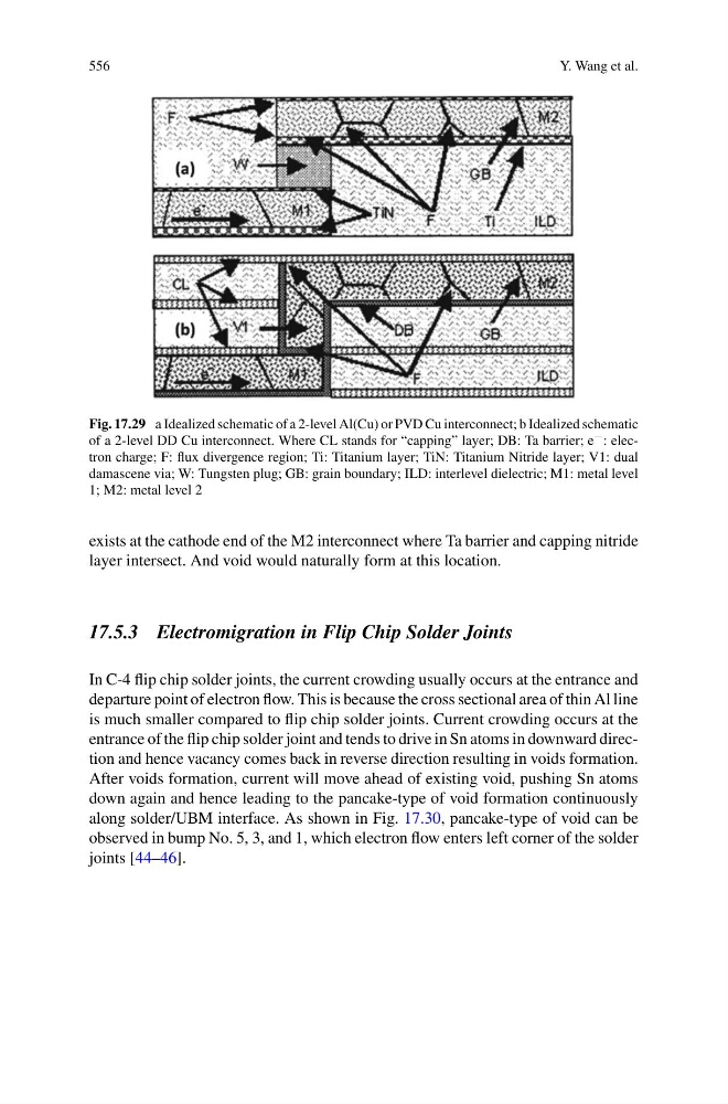
Fig. 17.29 a Idealized schematic of a 2-level Al(Cu) or PVD Cu interconnect; b Idealized schematic
of a 2-level DD Cu interconnect. Where CL stands for “capping” layer; DB: Ta barrier; e − : electron charge; F: flux divergence region; Ti: Titanium layer; TiN: Titanium Nitride layer; V1: dual
damascene via; W: Tungsten plug; GB: grain boundary; ILD: interlevel dielectric; M1: metal level
1; M2: metal level 2
exists at the cathode end of the M2 interconnect where Ta barrier and capping nitride
layer intersect. And void would naturally form at this location.
17.5.3 Electromigration in Flip Chip Solder Joints
In C-4 flip chip solder joints, the current crowding usually occurs at the entrance and
departure point of electron flow. This is because the cross sectional area of thin Al line
is much smaller compared to flip chip solder joints. Current crowding occurs at the
entrance of the flip chip solder joint and tends to drive in Sn atoms in downward direction and hence vacancy comes back in reverse direction resulting in voids formation.
After voids formation, current will move ahead of existing void, pushing Sn atoms
down again and hence leading to the pancake-type of void formation continuously
along solder/UBM interface. As shown in Fig. 17.30, pancake-type of void can be
observed in bump No. 5, 3, and 1, which electron flow enters left corner of the solder
joints [44–46].
Y. Wang et al.
Fig. 17.29 a Idealized schematic of a 2-level Al(Cu) or PVD Cu interconnect; b Idealized schematic
of a 2-level DD Cu interconnect. Where CL stands for “capping” layer; DB: Ta barrier; e − : electron charge; F: flux divergence region; Ti: Titanium layer; TiN: Titanium Nitride layer; V1: dual
damascene via; W: Tungsten plug; GB: grain boundary; ILD: interlevel dielectric; M1: metal level
1; M2: metal level 2
exists at the cathode end of the M2 interconnect where Ta barrier and capping nitride
layer intersect. And void would naturally form at this location.
17.5.3 Electromigration in Flip Chip Solder Joints
In C-4 flip chip solder joints, the current crowding usually occurs at the entrance and
departure point of electron flow. This is because the cross sectional area of thin Al line
is much smaller compared to flip chip solder joints. Current crowding occurs at the
entrance of the flip chip solder joint and tends to drive in Sn atoms in downward direction and hence vacancy comes back in reverse direction resulting in voids formation.
After voids formation, current will move ahead of existing void, pushing Sn atoms
down again and hence leading to the pancake-type of void formation continuously
along solder/UBM interface. As shown in Fig. 17.30, pancake-type of void can be
observed in bump No. 5, 3, and 1, which electron flow enters left corner of the solder
joints [44–46].