

17 Interconnect Quality and Reliability of 3D Packaging
553
were used. Electromigration (EM) in interconnects has been one of the most crucial
and persistent reliability issues in Si-based microelectronic technology. Al or Cu
interconnects usually have a small cross sectional area. Thus, a very high current
density will be carried, typically 10
5 –10
6 A/cm
2 . Under such high current density,
atomic diffusion and rearrangement are enhanced, leading to void formation at the
cathode and extrusion in the anode. The cathode and anode are sites of atomic flux
divergence, which has been recognized. The analysis of back stress accompanying
EM has also attracted much attention. When flip chip technology introduced the
C-4 solder joint, the effect of current crowding on EM was found to occur near
the contact area of solder joints with a current density about 10
4 A/cm
2 [1–4, 30–
34]. As consumer electronic products is ubiquitous in the big data era, its dense
packaging in using very small size microbumps in 2.5D/3D IC requires a careful
thermal management. While EM damage is still affected by flux divergence, backstress, and current crowding, Joule heating is now the new focus.
After introducing the basic concepts in electromigration very briefly below, we
will show experimental findings of EM damages in interconnects and flip chip solder
joints. Then we will discuss EM failures of 3D IC in using the vertical stacking of
Si chips containing the new interconnect structure of microbumps and TSVs. Based
on these new structures, we will present their EM behaviors. Especially, we show
that system level EM study is becoming important. In the system, a surprise was
the failure of the redistribution layer (RDL) between the C-4 solder joints and the
microbumps. In the system level EM test, heat dissipation becomes a critical problem.
Synergistic effect of Joule heating and EM will be discussed.
17.5.1 Introduction on Electromigration
Electromigration is the interaction between electron flow and atomic diffusion. The
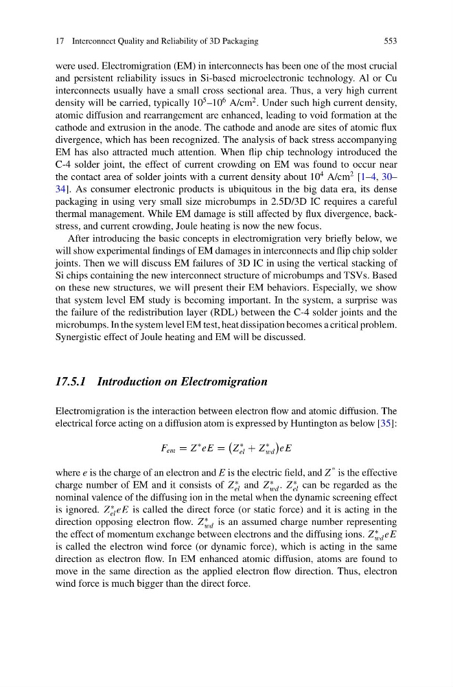
electrical force acting on a diffusion atom is expressed by Huntington as below [35]:
F em = Z
∗ eE =
Z
∗
el + Z
∗
wd
eE
where e is the charge of an electron and E is the electric field, and Z
* is the effective
charge number of EM and it consists of Z
∗
el and Z
∗
wd . Z
∗
el can be regarded as the
nominal valence of the diffusing ion in the metal when the dynamic screening effect
is ignored. Z
∗
el eE is called the direct force (or static force) and it is acting in the
direction opposing electron flow. Z
∗
wd is an assumed charge number representing
the effect of momentum exchange between electrons and the diffusing ions. Z
∗
wd eE
is called the electron wind force (or dynamic force), which is acting in the same
direction as electron flow. In EM enhanced atomic diffusion, atoms are found to
move in the same direction as the applied electron flow direction. Thus, electron
wind force is much bigger than the direct force.
553
were used. Electromigration (EM) in interconnects has been one of the most crucial
and persistent reliability issues in Si-based microelectronic technology. Al or Cu
interconnects usually have a small cross sectional area. Thus, a very high current
density will be carried, typically 10
5 –10
6 A/cm
2 . Under such high current density,
atomic diffusion and rearrangement are enhanced, leading to void formation at the
cathode and extrusion in the anode. The cathode and anode are sites of atomic flux
divergence, which has been recognized. The analysis of back stress accompanying
EM has also attracted much attention. When flip chip technology introduced the
C-4 solder joint, the effect of current crowding on EM was found to occur near
the contact area of solder joints with a current density about 10
4 A/cm
2 [1–4, 30–
34]. As consumer electronic products is ubiquitous in the big data era, its dense
packaging in using very small size microbumps in 2.5D/3D IC requires a careful
thermal management. While EM damage is still affected by flux divergence, backstress, and current crowding, Joule heating is now the new focus.
After introducing the basic concepts in electromigration very briefly below, we
will show experimental findings of EM damages in interconnects and flip chip solder
joints. Then we will discuss EM failures of 3D IC in using the vertical stacking of
Si chips containing the new interconnect structure of microbumps and TSVs. Based
on these new structures, we will present their EM behaviors. Especially, we show
that system level EM study is becoming important. In the system, a surprise was
the failure of the redistribution layer (RDL) between the C-4 solder joints and the
microbumps. In the system level EM test, heat dissipation becomes a critical problem.
Synergistic effect of Joule heating and EM will be discussed.
17.5.1 Introduction on Electromigration
Electromigration is the interaction between electron flow and atomic diffusion. The
electrical force acting on a diffusion atom is expressed by Huntington as below [35]:
F em = Z
∗ eE =
Z
∗
el + Z
∗
wd
eE
where e is the charge of an electron and E is the electric field, and Z
* is the effective
charge number of EM and it consists of Z
∗
el and Z
∗
wd . Z
∗
el can be regarded as the
nominal valence of the diffusing ion in the metal when the dynamic screening effect
is ignored. Z
∗
el eE is called the direct force (or static force) and it is acting in the
direction opposing electron flow. Z
∗
wd is an assumed charge number representing
the effect of momentum exchange between electrons and the diffusing ions. Z
∗
wd eE
is called the electron wind force (or dynamic force), which is acting in the same
direction as electron flow. In EM enhanced atomic diffusion, atoms are found to
move in the same direction as the applied electron flow direction. Thus, electron
wind force is much bigger than the direct force.