

548
Y. Wang et al.
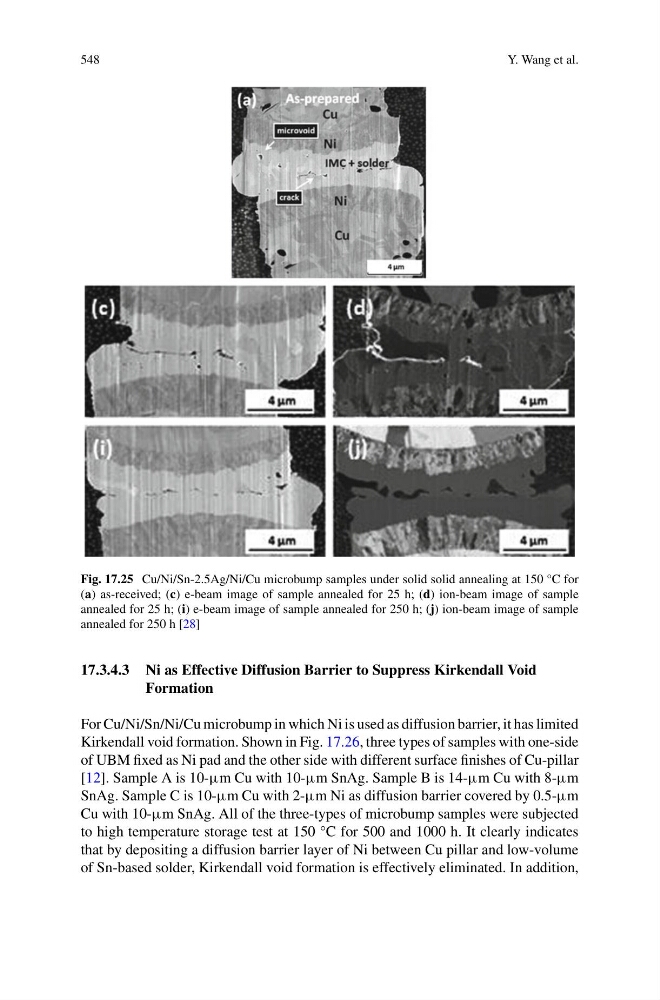
Fig. 17.25 Cu/Ni/Sn-2.5Ag/Ni/Cu microbump samples under solid solid annealing at 150 °C for
(a) as-received; (c) e-beam image of sample annealed for 25 h; (d) ion-beam image of sample
annealed for 25 h; (i) e-beam image of sample annealed for 250 h; (j) ion-beam image of sample
annealed for 250 h [28]
17.3.4.3 Ni as Effective Diffusion Barrier to Suppress Kirkendall Void
Formation
For Cu/Ni/Sn/Ni/Cu microbump in which Ni is used as diffusion barrier, it has limited
Kirkendall void formation. Shown in Fig. 17.26, three types of samples with one-side
of UBM fixed as Ni pad and the other side with different surface finishes of Cu-pillar
[12]. Sample A is 10-μm Cu with 10-μm SnAg. Sample B is 14-μm Cu with 8-μm
SnAg. Sample C is 10-μm Cu with 2-μm Ni as diffusion barrier covered by 0.5-μm
Cu with 10-μm SnAg. All of the three-types of microbump samples were subjected
to high temperature storage test at 150 °C for 500 and 1000 h. It clearly indicates
that by depositing a diffusion barrier layer of Ni between Cu pillar and low-volume
of Sn-based solder, Kirkendall void formation is effectively eliminated. In addition,
Y. Wang et al.
Fig. 17.25 Cu/Ni/Sn-2.5Ag/Ni/Cu microbump samples under solid solid annealing at 150 °C for
(a) as-received; (c) e-beam image of sample annealed for 25 h; (d) ion-beam image of sample
annealed for 25 h; (i) e-beam image of sample annealed for 250 h; (j) ion-beam image of sample
annealed for 250 h [28]
17.3.4.3 Ni as Effective Diffusion Barrier to Suppress Kirkendall Void
Formation
For Cu/Ni/Sn/Ni/Cu microbump in which Ni is used as diffusion barrier, it has limited
Kirkendall void formation. Shown in Fig. 17.26, three types of samples with one-side
of UBM fixed as Ni pad and the other side with different surface finishes of Cu-pillar
[12]. Sample A is 10-μm Cu with 10-μm SnAg. Sample B is 14-μm Cu with 8-μm
SnAg. Sample C is 10-μm Cu with 2-μm Ni as diffusion barrier covered by 0.5-μm
Cu with 10-μm SnAg. All of the three-types of microbump samples were subjected
to high temperature storage test at 150 °C for 500 and 1000 h. It clearly indicates
that by depositing a diffusion barrier layer of Ni between Cu pillar and low-volume
of Sn-based solder, Kirkendall void formation is effectively eliminated. In addition,