

546
Y. Wang et al.
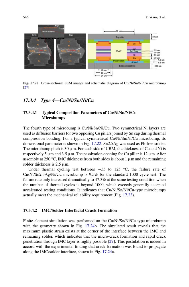
Fig. 17.22 Cross-sectional SEM images and schematic diagram of Cu/Ni/Sn/Ni/Cu microbump
[27]
17.3.4 Type 4—Cu/Ni/Sn/Ni/Cu
17.3.4.1 Typical Composition Parameters of Cu/Ni/Sn/Ni/Cu
Microbumps
The fourth type of microbump is Cu/Ni/Sn/Ni/Cu. Two symmetrical Ni layers are
used as diffusion barriers for two opposing Cu pillars joined by Sn cap during thermal
compression bonding. For a typical symmetrical Cu/Ni/Sn/Ni/Cu microbump, its
dimensional parameter is shown in Fig. 17.22. Sn2.5Ag was used as Pb-free solder.
The microbump pitch is 30 μm. For each side of UBM, the thickness of Cu and Ni is
respectively 5 μm and 3.5 μm. The passivation opening for Cu pillar is 12 μm. After
assembly at 250 °C, IMC thickness from both sides is about 1 μm and the remaining
solder thickness is 2.5 μm.
Under thermal cycling test between −55 to 125 °C, the failure rate of
Cu/Ni/Sn2.5Ag/Ni/Cu microbump is 9.5% for the standard 1000 cycle test. The
failure rate only increased dramatically to 47.3% at the same testing condition when
the number of thermal cycles is beyond 1000, which exceeds generally accepted
accelerated testing conditions. It indicates that Cu/Ni/Sn/Ni/Cu-type microbumps
actually meet the mechanical reliability requirement (Fig. 17.23).
17.3.4.2 IMC/Solder Interfacial Crack Formation
Finite element simulation was performed on the Cu/Ni/Sn/Ni/Cu-type microbump
with the geometry shown in Fig. 17.24b. The simulated result reveals that the
maximum plastic strain exists at the corner of the interface between the IMC and
remaining solder, which indicates that the micro-crack formation and rapid crack
penetration through IMC layer is highly possible [27]. This postulation is indeed in
accord with the experimental finding that crack formation was found to propagate
along the IMC/solder interface, shown in Fig. 17.24a.
Y. Wang et al.
Fig. 17.22 Cross-sectional SEM images and schematic diagram of Cu/Ni/Sn/Ni/Cu microbump
[27]
17.3.4 Type 4—Cu/Ni/Sn/Ni/Cu
17.3.4.1 Typical Composition Parameters of Cu/Ni/Sn/Ni/Cu
Microbumps
The fourth type of microbump is Cu/Ni/Sn/Ni/Cu. Two symmetrical Ni layers are
used as diffusion barriers for two opposing Cu pillars joined by Sn cap during thermal
compression bonding. For a typical symmetrical Cu/Ni/Sn/Ni/Cu microbump, its
dimensional parameter is shown in Fig. 17.22. Sn2.5Ag was used as Pb-free solder.
The microbump pitch is 30 μm. For each side of UBM, the thickness of Cu and Ni is
respectively 5 μm and 3.5 μm. The passivation opening for Cu pillar is 12 μm. After
assembly at 250 °C, IMC thickness from both sides is about 1 μm and the remaining
solder thickness is 2.5 μm.
Under thermal cycling test between −55 to 125 °C, the failure rate of
Cu/Ni/Sn2.5Ag/Ni/Cu microbump is 9.5% for the standard 1000 cycle test. The
failure rate only increased dramatically to 47.3% at the same testing condition when
the number of thermal cycles is beyond 1000, which exceeds generally accepted
accelerated testing conditions. It indicates that Cu/Ni/Sn/Ni/Cu-type microbumps
actually meet the mechanical reliability requirement (Fig. 17.23).
17.3.4.2 IMC/Solder Interfacial Crack Formation
Finite element simulation was performed on the Cu/Ni/Sn/Ni/Cu-type microbump
with the geometry shown in Fig. 17.24b. The simulated result reveals that the
maximum plastic strain exists at the corner of the interface between the IMC and
remaining solder, which indicates that the micro-crack formation and rapid crack
penetration through IMC layer is highly possible [27]. This postulation is indeed in
accord with the experimental finding that crack formation was found to propagate
along the IMC/solder interface, shown in Fig. 17.24a.