

17 Interconnect Quality and Reliability of 3D Packaging
545
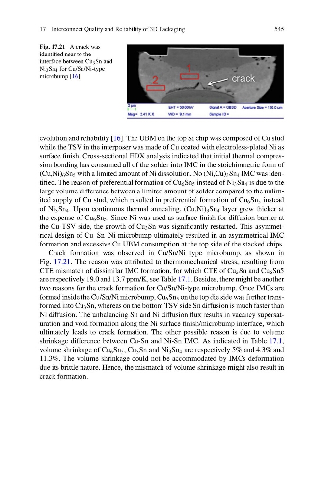
Fig. 17.21 A crack was
identified near to the
interface between Cu 3 Sn and
Ni 3 Sn 4 for Cu/Sn/Ni-type
microbump [16]
evolution and reliability [16]. The UBM on the top Si chip was composed of Cu stud
while the TSV in the interposer was made of Cu coated with electroless-plated Ni as
surface finish. Cross-sectional EDX analysis indicated that initial thermal compression bonding has consumed all of the solder into IMC in the stoichiometric form of
(Cu,Ni) 6 Sn 5 with a limited amount of Ni dissolution. No (Ni,Cu) 3 Sn 4 IMC was identified. The reason of preferential formation of Cu 6 Sn 5 instead of Ni 3 Sn 4 is due to the
large volume difference between a limited amount of solder compared to the unlimited supply of Cu stud, which resulted in preferential formation of Cu 6 Sn 5 instead
of Ni 3 Sn 4 . Upon continuous thermal annealing, (Cu,Ni) 3 Sn 4 layer grew thicker at
the expense of Cu 6 Sn 5 . Since Ni was used as surface finish for diffusion barrier at
the Cu-TSV side, the growth of Cu 3 Sn was significantly restarted. This asymmetrical design of Cu–Sn–Ni microbump ultimately resulted in an asymmetrical IMC
formation and excessive Cu UBM consumption at the top side of the stacked chips.
Crack formation was observed in Cu/Sn/Ni type microbump, as shown in
Fig. 17.21. The reason was attributed to thermomechanical stress, resulting from
CTE mismatch of dissimilar IMC formation, for which CTE of Cu 3 Sn and Cu 6 Sn5
are respectively 19.0 and 13.7 ppm/K, see Table 17.1. Besides, there might be another
two reasons for the crack formation for Cu/Sn/Ni-type microbump. Once IMCs are
formed inside the Cu/Sn/Ni microbump, Cu 6 Sn 5 on the top die side was further transformed into Cu 3 Sn, whereas on the bottom TSV side Sn diffusion is much faster than
Ni diffusion. The unbalancing Sn and Ni diffusion flux results in vacancy supersaturation and void formation along the Ni surface finish/microbump interface, which
ultimately leads to crack formation. The other possible reason is due to volume
shrinkage difference between Cu-Sn and Ni-Sn IMC. As indicated in Table 17.1,
volume shrinkage of Cu 6 Sn 5 , Cu 3 Sn and Ni 3 Sn 4 are respectively 5% and 4.3% and
11.3%. The volume shrinkage could not be accommodated by IMCs deformation
due its brittle nature. Hence, the mismatch of volume shrinkage might also result in
crack formation.
545
Fig. 17.21 A crack was
identified near to the
interface between Cu 3 Sn and
Ni 3 Sn 4 for Cu/Sn/Ni-type
microbump [16]
evolution and reliability [16]. The UBM on the top Si chip was composed of Cu stud
while the TSV in the interposer was made of Cu coated with electroless-plated Ni as
surface finish. Cross-sectional EDX analysis indicated that initial thermal compression bonding has consumed all of the solder into IMC in the stoichiometric form of
(Cu,Ni) 6 Sn 5 with a limited amount of Ni dissolution. No (Ni,Cu) 3 Sn 4 IMC was identified. The reason of preferential formation of Cu 6 Sn 5 instead of Ni 3 Sn 4 is due to the
large volume difference between a limited amount of solder compared to the unlimited supply of Cu stud, which resulted in preferential formation of Cu 6 Sn 5 instead
of Ni 3 Sn 4 . Upon continuous thermal annealing, (Cu,Ni) 3 Sn 4 layer grew thicker at
the expense of Cu 6 Sn 5 . Since Ni was used as surface finish for diffusion barrier at
the Cu-TSV side, the growth of Cu 3 Sn was significantly restarted. This asymmetrical design of Cu–Sn–Ni microbump ultimately resulted in an asymmetrical IMC
formation and excessive Cu UBM consumption at the top side of the stacked chips.
Crack formation was observed in Cu/Sn/Ni type microbump, as shown in
Fig. 17.21. The reason was attributed to thermomechanical stress, resulting from
CTE mismatch of dissimilar IMC formation, for which CTE of Cu 3 Sn and Cu 6 Sn5
are respectively 19.0 and 13.7 ppm/K, see Table 17.1. Besides, there might be another
two reasons for the crack formation for Cu/Sn/Ni-type microbump. Once IMCs are
formed inside the Cu/Sn/Ni microbump, Cu 6 Sn 5 on the top die side was further transformed into Cu 3 Sn, whereas on the bottom TSV side Sn diffusion is much faster than
Ni diffusion. The unbalancing Sn and Ni diffusion flux results in vacancy supersaturation and void formation along the Ni surface finish/microbump interface, which
ultimately leads to crack formation. The other possible reason is due to volume
shrinkage difference between Cu-Sn and Ni-Sn IMC. As indicated in Table 17.1,
volume shrinkage of Cu 6 Sn 5 , Cu 3 Sn and Ni 3 Sn 4 are respectively 5% and 4.3% and
11.3%. The volume shrinkage could not be accommodated by IMCs deformation
due its brittle nature. Hence, the mismatch of volume shrinkage might also result in
crack formation.