

544
Y. Wang et al.
microbump annealed at 180 °C for 240 h was identified. The cross-section was
polished by ion beam milling to avoid possible mechanical polishing induced microcrack formation or polishing powder smearing effect. Figure 17.19 clearly demonstrates that the void was originated from Sn pockets during Ni/Sn IMC formation.
As also indicated by Chen’s Ph.D. thesis [26], for Ni–Sn–Ni microbump, Sn is faster
diffusion species compared to Ni. The IMC growth during thermal annealing is also
a flux-driven ripening process, which means larger grains will grow at the expense of
smaller grains. The ripening effect tends to result in uneven interface due to opposing
IMC impingement and hence result in forming Sn pockets in thermal annealing.
Since Sn is faster diffusion species, the asymmetrical atomic flux results in vacancy
accumulate inside Sn pocket. When the remaining Sn is completely consumed, the
supersaturation of vacancy leads to void formation and therefore trapped inside the
original position of Sn pocket. No doubt, the void trapped inside Ni 3 Sn 4 -microbump
can adversely degrade IMC mechanical reliability. In terms of UBM used for Ni 3 Sn 4 -
microbump, in which Ni (E = 186 GPa) itself is less mechanically compliant than
Cu (E = 120 GPa), see Table 17.1. It seems that Ni 3 Sn 4 microbump, based on the
above discussion, would have a more serious mechanical reliability concerns than
Cu-based microbumps: the trapped impurities induced grain boundaries embrittlement and volume shrinkage resulted void or micro-crack formation. Traditionally, Ni
was introduced to reduce IMC formation in order to address mechanical reliability
concerns. Nevertheless, for the application of fine-pitch interconnects in 3D IC technology which requires joint thickness down to 5 μm, joint with full IMC formation
is inevitable so that the utilization of Ni as UBM would not necessarily mitigate the
full IMC formation and might actually result in serious mechanical reliability issues.
17.3.3 Type 3—Cu/Sn/Ni
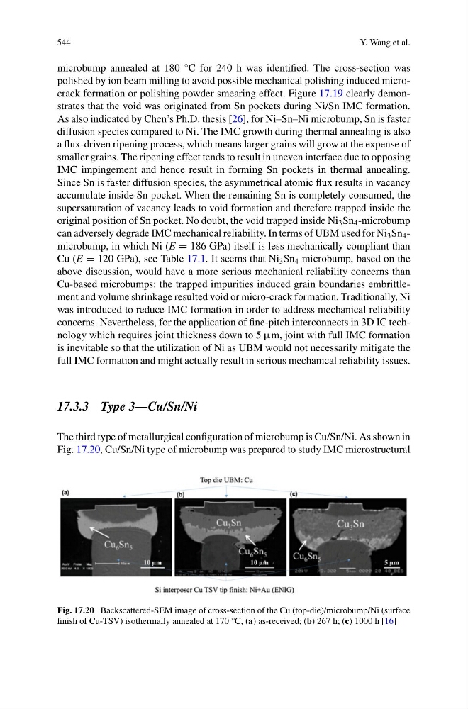
The third type of metallurgical configuration of microbump is Cu/Sn/Ni. As shown in
Fig. 17.20, Cu/Sn/Ni type of microbump was prepared to study IMC microstructural
Fig. 17.20 Backscattered-SEM image of cross-section of the Cu (top-die)/microbump/Ni (surface
finish of Cu-TSV) isothermally annealed at 170 °C, (a) as-received; (b) 267 h; (c) 1000 h [16]
Y. Wang et al.
microbump annealed at 180 °C for 240 h was identified. The cross-section was
polished by ion beam milling to avoid possible mechanical polishing induced microcrack formation or polishing powder smearing effect. Figure 17.19 clearly demonstrates that the void was originated from Sn pockets during Ni/Sn IMC formation.
As also indicated by Chen’s Ph.D. thesis [26], for Ni–Sn–Ni microbump, Sn is faster
diffusion species compared to Ni. The IMC growth during thermal annealing is also
a flux-driven ripening process, which means larger grains will grow at the expense of
smaller grains. The ripening effect tends to result in uneven interface due to opposing
IMC impingement and hence result in forming Sn pockets in thermal annealing.
Since Sn is faster diffusion species, the asymmetrical atomic flux results in vacancy
accumulate inside Sn pocket. When the remaining Sn is completely consumed, the
supersaturation of vacancy leads to void formation and therefore trapped inside the
original position of Sn pocket. No doubt, the void trapped inside Ni 3 Sn 4 -microbump
can adversely degrade IMC mechanical reliability. In terms of UBM used for Ni 3 Sn 4 -
microbump, in which Ni (E = 186 GPa) itself is less mechanically compliant than
Cu (E = 120 GPa), see Table 17.1. It seems that Ni 3 Sn 4 microbump, based on the
above discussion, would have a more serious mechanical reliability concerns than
Cu-based microbumps: the trapped impurities induced grain boundaries embrittlement and volume shrinkage resulted void or micro-crack formation. Traditionally, Ni
was introduced to reduce IMC formation in order to address mechanical reliability
concerns. Nevertheless, for the application of fine-pitch interconnects in 3D IC technology which requires joint thickness down to 5 μm, joint with full IMC formation
is inevitable so that the utilization of Ni as UBM would not necessarily mitigate the
full IMC formation and might actually result in serious mechanical reliability issues.
17.3.3 Type 3—Cu/Sn/Ni
The third type of metallurgical configuration of microbump is Cu/Sn/Ni. As shown in
Fig. 17.20, Cu/Sn/Ni type of microbump was prepared to study IMC microstructural
Fig. 17.20 Backscattered-SEM image of cross-section of the Cu (top-die)/microbump/Ni (surface
finish of Cu-TSV) isothermally annealed at 170 °C, (a) as-received; (b) 267 h; (c) 1000 h [16]