

17 Interconnect Quality and Reliability of 3D Packaging
543
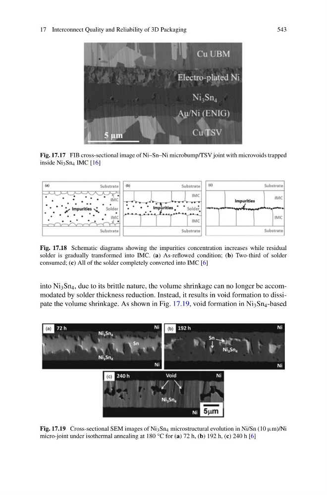
Fig. 17.17 FIB cross-sectional image of Ni–Sn–Ni microbump/TSV joint with microvoids trapped
inside Ni 3 Sn 4 IMC [16]
Fig. 17.18 Schematic diagrams showing the impurities concentration increases while residual
solder is gradually transformed into IMC. (a) As-reflowed condition; (b) Two-third of solder
consumed; (c) All of the solder completely converted into IMC [6]
into Ni 3 Sn 4 , due to its brittle nature, the volume shrinkage can no longer be accommodated by solder thickness reduction. Instead, it results in void formation to dissipate the volume shrinkage. As shown in Fig. 17.19, void formation in Ni 3 Sn 4 -based
Fig. 17.19 Cross-sectional SEM images of Ni 3 Sn 4 microstructural evolution in Ni/Sn (10 μm)/Ni
micro-joint under isothermal annealing at 180 °C for (a) 72 h, (b) 192 h, (c) 240 h [6]
543
Fig. 17.17 FIB cross-sectional image of Ni–Sn–Ni microbump/TSV joint with microvoids trapped
inside Ni 3 Sn 4 IMC [16]
Fig. 17.18 Schematic diagrams showing the impurities concentration increases while residual
solder is gradually transformed into IMC. (a) As-reflowed condition; (b) Two-third of solder
consumed; (c) All of the solder completely converted into IMC [6]
into Ni 3 Sn 4 , due to its brittle nature, the volume shrinkage can no longer be accommodated by solder thickness reduction. Instead, it results in void formation to dissipate the volume shrinkage. As shown in Fig. 17.19, void formation in Ni 3 Sn 4 -based
Fig. 17.19 Cross-sectional SEM images of Ni 3 Sn 4 microstructural evolution in Ni/Sn (10 μm)/Ni
micro-joint under isothermal annealing at 180 °C for (a) 72 h, (b) 192 h, (c) 240 h [6]