

542
Y. Wang et al.
has highest joint shear strength [24]. This unique oriented growth of Cu 6 Sn 5 is worth
to be further studied and applied in a controlled growth of IMC-based microbump.
17.3.2 Type 2—Ni/Sn/Ni
For typical Ni/Sn/Ni microbump, Ni is used as diffusion barrier to retard IMC formation especially under reflow or thermal compression bonding. Hence, it could leave
behind a sufficient amount of un-reacted solder as mechanical buffer layer to retain the
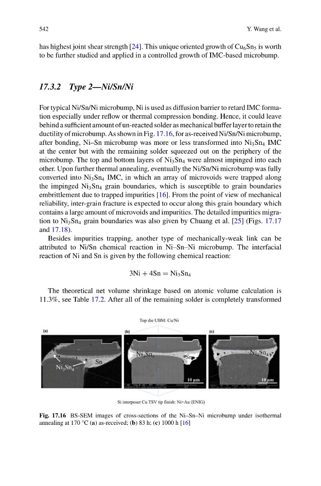
ductility of microbump. As shown in Fig. 17.16, for as-received Ni/Sn/Ni microbump,
after bonding, Ni–Sn microbump was more or less transformed into Ni 3 Sn 4 IMC
at the center but with the remaining solder squeezed out on the periphery of the
microbump. The top and bottom layers of Ni 3 Sn 4 were almost impinged into each
other. Upon further thermal annealing, eventually the Ni/Sn/Ni microbump was fully
converted into Ni 3 Sn 4 IMC, in which an array of microvoids were trapped along
the impinged Ni 3 Sn 4 grain boundaries, which is susceptible to grain boundaries
embrittlement due to trapped impurities [16]. From the point of view of mechanical
reliability, inter-grain fracture is expected to occur along this grain boundary which
contains a large amount of microvoids and impurities. The detailed impurities migration to Ni 3 Sn 4 grain boundaries was also given by Chuang et al. [25] (Figs. 17.17
and 17.18).
Besides impurities trapping, another type of mechanically-weak link can be
attributed to Ni/Sn chemical reaction in Ni–Sn–Ni microbump. The interfacial
reaction of Ni and Sn is given by the following chemical reaction:
3Ni + 4Sn = Ni 3 Sn 4
The theoretical net volume shrinkage based on atomic volume calculation is
11.3%, see Table 17.2. After all of the remaining solder is completely transformed
Fig. 17.16 BS-SEM images of cross-sections of the Ni–Sn–Ni microbump under isothermal
annealing at 170 °C (a) as-received; (b) 83 h; (c) 1000 h [16]
Y. Wang et al.
has highest joint shear strength [24]. This unique oriented growth of Cu 6 Sn 5 is worth
to be further studied and applied in a controlled growth of IMC-based microbump.
17.3.2 Type 2—Ni/Sn/Ni
For typical Ni/Sn/Ni microbump, Ni is used as diffusion barrier to retard IMC formation especially under reflow or thermal compression bonding. Hence, it could leave
behind a sufficient amount of un-reacted solder as mechanical buffer layer to retain the
ductility of microbump. As shown in Fig. 17.16, for as-received Ni/Sn/Ni microbump,
after bonding, Ni–Sn microbump was more or less transformed into Ni 3 Sn 4 IMC
at the center but with the remaining solder squeezed out on the periphery of the
microbump. The top and bottom layers of Ni 3 Sn 4 were almost impinged into each
other. Upon further thermal annealing, eventually the Ni/Sn/Ni microbump was fully
converted into Ni 3 Sn 4 IMC, in which an array of microvoids were trapped along
the impinged Ni 3 Sn 4 grain boundaries, which is susceptible to grain boundaries
embrittlement due to trapped impurities [16]. From the point of view of mechanical
reliability, inter-grain fracture is expected to occur along this grain boundary which
contains a large amount of microvoids and impurities. The detailed impurities migration to Ni 3 Sn 4 grain boundaries was also given by Chuang et al. [25] (Figs. 17.17
and 17.18).
Besides impurities trapping, another type of mechanically-weak link can be
attributed to Ni/Sn chemical reaction in Ni–Sn–Ni microbump. The interfacial
reaction of Ni and Sn is given by the following chemical reaction:
3Ni + 4Sn = Ni 3 Sn 4
The theoretical net volume shrinkage based on atomic volume calculation is
11.3%, see Table 17.2. After all of the remaining solder is completely transformed
Fig. 17.16 BS-SEM images of cross-sections of the Ni–Sn–Ni microbump under isothermal
annealing at 170 °C (a) as-received; (b) 83 h; (c) 1000 h [16]