

17 Interconnect Quality and Reliability of 3D Packaging
537
that Kirkendall voids were preferentially nucleated at the Cu/Cu 3 Sn interface because
of heterogeneous nucleation. This was suggested to be the reason why Kirkendall
void formation was only observed on the Cu-TSV interface instead of on the chip
side [16] (Fig. 17.8).
Besides Kirkendall void formation, Chen et al. recently reported that there is
another type of porous void formation which can happen inside Cu/Cu 3 Sn/Cu
microbump under aggressive thermal annealing or current stressing [17–19]. In
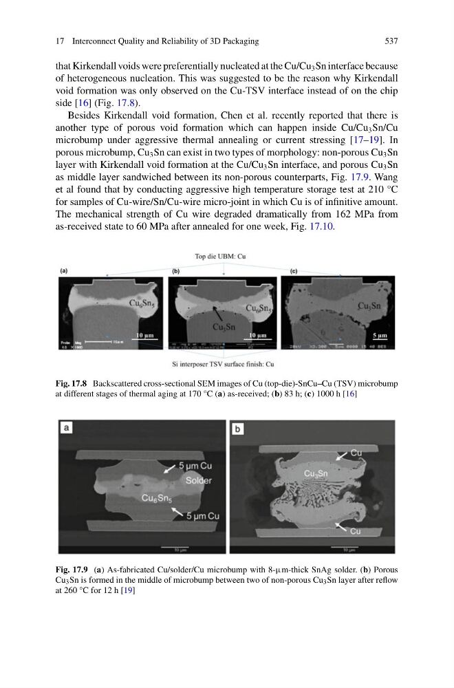
porous microbump, Cu 3 Sn can exist in two types of morphology: non-porous Cu 3 Sn
layer with Kirkendall void formation at the Cu/Cu 3 Sn interface, and porous Cu 3 Sn
as middle layer sandwiched between its non-porous counterparts, Fig. 17.9. Wang
et al found that by conducting aggressive high temperature storage test at 210 °C
for samples of Cu-wire/Sn/Cu-wire micro-joint in which Cu is of infinitive amount.
The mechanical strength of Cu wire degraded dramatically from 162 MPa from
as-received state to 60 MPa after annealed for one week, Fig. 17.10.
Fig. 17.8 Backscattered cross-sectional SEM images of Cu (top-die)-SnCu–Cu (TSV) microbump
at different stages of thermal aging at 170 °C (a) as-received; (b) 83 h; (c) 1000 h [16]
Fig. 17.9 (a) As-fabricated Cu/solder/Cu microbump with 8-μm-thick SnAg solder. (b) Porous
Cu 3 Sn is formed in the middle of microbump between two of non-porous Cu 3 Sn layer after reflow
at 260 °C for 12 h [19]
537
that Kirkendall voids were preferentially nucleated at the Cu/Cu 3 Sn interface because
of heterogeneous nucleation. This was suggested to be the reason why Kirkendall
void formation was only observed on the Cu-TSV interface instead of on the chip
side [16] (Fig. 17.8).
Besides Kirkendall void formation, Chen et al. recently reported that there is
another type of porous void formation which can happen inside Cu/Cu 3 Sn/Cu
microbump under aggressive thermal annealing or current stressing [17–19]. In
porous microbump, Cu 3 Sn can exist in two types of morphology: non-porous Cu 3 Sn
layer with Kirkendall void formation at the Cu/Cu 3 Sn interface, and porous Cu 3 Sn
as middle layer sandwiched between its non-porous counterparts, Fig. 17.9. Wang
et al found that by conducting aggressive high temperature storage test at 210 °C
for samples of Cu-wire/Sn/Cu-wire micro-joint in which Cu is of infinitive amount.
The mechanical strength of Cu wire degraded dramatically from 162 MPa from
as-received state to 60 MPa after annealed for one week, Fig. 17.10.
Fig. 17.8 Backscattered cross-sectional SEM images of Cu (top-die)-SnCu–Cu (TSV) microbump
at different stages of thermal aging at 170 °C (a) as-received; (b) 83 h; (c) 1000 h [16]
Fig. 17.9 (a) As-fabricated Cu/solder/Cu microbump with 8-μm-thick SnAg solder. (b) Porous
Cu 3 Sn is formed in the middle of microbump between two of non-porous Cu 3 Sn layer after reflow
at 260 °C for 12 h [19]