

536
Y. Wang et al.
formation in the Cu 3 Sn layer [8, 9]. Kirkendall void formation is due to unbalancing
interdiffusion of Cu and Sn atomic flux where Cu diffuses much faster than Sn in
the reverse direction [8, 10]. However, Kirkendall void can be effectively reduced by
adding Co or Ni into Pb-free solder [11]. Besides, by controlling electroplating bath,
or to have nano-twinned Cu as UBM can significantly reduce micro-void nucleation
[12–15]. Kirkendall void can be a serious reliability issue. If it is not under control,
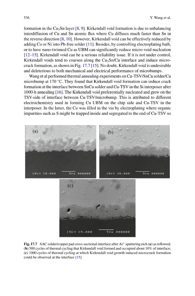
Kirkendall voids tend to coarsen along the Cu 3 Sn/Cu interface and induce microcrack formation, as shown in Fig. 17.7 [15]. No doubt, Kirkendall void is undesirable
and deleterious to both mechanical and electrical performance of microbumps.
Wang et al performed thermal annealing experiments on Cu-TSV/SnCu solder/Cu
microbump at 170 °C. They found that Kirkendall void formation can induce crack
formation at the interface between SnCu solder and Cu-TSV in the Si interposer after
1000-h annealing [16]. The Kirkendall void preferentially nucleated and grew on the
TSV-side of interface between Cu-TSV/microbump. This is attributed to different
electrochemistry used in forming Cu UBM on the chip side and Cu-TSV in the
interposer. In the latter, the Cu was filled in the via by electroplating where organic
impurities such as S might be trapped inside and segregated to the end of Cu-TSV so
Fig. 17.7 SAC solder/copper pad cross-sectional interface after Ar + sputtering etch (a) as reflowed;
(b) 500 cycles of thermal cycling that Kirkendall void formed and occupied about 10% of interface;
(c) 1000 cycles of thermal cycling at which Kirkendall void growth induced microcrack formation
could be observed at the interface [15]
Y. Wang et al.
formation in the Cu 3 Sn layer [8, 9]. Kirkendall void formation is due to unbalancing
interdiffusion of Cu and Sn atomic flux where Cu diffuses much faster than Sn in
the reverse direction [8, 10]. However, Kirkendall void can be effectively reduced by
adding Co or Ni into Pb-free solder [11]. Besides, by controlling electroplating bath,
or to have nano-twinned Cu as UBM can significantly reduce micro-void nucleation
[12–15]. Kirkendall void can be a serious reliability issue. If it is not under control,
Kirkendall voids tend to coarsen along the Cu 3 Sn/Cu interface and induce microcrack formation, as shown in Fig. 17.7 [15]. No doubt, Kirkendall void is undesirable
and deleterious to both mechanical and electrical performance of microbumps.
Wang et al performed thermal annealing experiments on Cu-TSV/SnCu solder/Cu
microbump at 170 °C. They found that Kirkendall void formation can induce crack
formation at the interface between SnCu solder and Cu-TSV in the Si interposer after
1000-h annealing [16]. The Kirkendall void preferentially nucleated and grew on the
TSV-side of interface between Cu-TSV/microbump. This is attributed to different
electrochemistry used in forming Cu UBM on the chip side and Cu-TSV in the
interposer. In the latter, the Cu was filled in the via by electroplating where organic
impurities such as S might be trapped inside and segregated to the end of Cu-TSV so
Fig. 17.7 SAC solder/copper pad cross-sectional interface after Ar + sputtering etch (a) as reflowed;
(b) 500 cycles of thermal cycling that Kirkendall void formed and occupied about 10% of interface;
(c) 1000 cycles of thermal cycling at which Kirkendall void growth induced microcrack formation
could be observed at the interface [15]