

518
P. Vianco and M. Neilsen
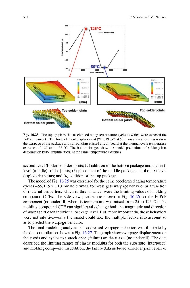
Fig. 16.23 The top graph is the accelerated aging temperature cycle to which were exposed the
PoP components. The finite element displacement (“DISPL_Z” at 50 × magnification) maps show
the warpage of the package and surrounding printed circuit board at the thermal cycle temperature
extremes of 125 and −55 °C. The bottom images show the model predictions of solder joints
deformation (50× amplification) at the same temperature extremes
second-level (bottom) solder joints; (2) addition of the bottom package and the firstlevel (middle) solder joints; (3) placement of the middle package and the first-level
(top) solder joints; and (4) addition of the top package.
The model of Fig. 16.25 was exercised for the same accelerated aging temperature
cycle (−55/125 °C; 10 min hold times) to investigate warpage behavior as a function
of material properties, which in this instance, were the limiting values of molding
compound CTEs. The side-view profiles are shown in Fig. 16.26 for the PoPoP
component (no underfill) when its temperature was raised from 25 to 125 °C. The
molding compound CTE can significantly change both the magnitude and direction
of warpage at each individual package level. But, more importantly, those behaviors
were not intuitive—only the model could take the multiple factors into account so
as to predict the warpage behavior.
The final modeling analysis that addressed warpage behavior, was illustrate by
the data compilation shown in Fig. 16.27. The graph shows warpage displacement on
the y-axis and cycles to a crack open (failure) on the x-axis (no underfill). The data
described the limiting ranges of elastic modulus for both the substrate (interposer)
and molding compound. In addition, the failure data included all solder joint levels of
P. Vianco and M. Neilsen
Fig. 16.23 The top graph is the accelerated aging temperature cycle to which were exposed the
PoP components. The finite element displacement (“DISPL_Z” at 50 × magnification) maps show
the warpage of the package and surrounding printed circuit board at the thermal cycle temperature
extremes of 125 and −55 °C. The bottom images show the model predictions of solder joints
deformation (50× amplification) at the same temperature extremes
second-level (bottom) solder joints; (2) addition of the bottom package and the firstlevel (middle) solder joints; (3) placement of the middle package and the first-level
(top) solder joints; and (4) addition of the top package.
The model of Fig. 16.25 was exercised for the same accelerated aging temperature
cycle (−55/125 °C; 10 min hold times) to investigate warpage behavior as a function
of material properties, which in this instance, were the limiting values of molding
compound CTEs. The side-view profiles are shown in Fig. 16.26 for the PoPoP
component (no underfill) when its temperature was raised from 25 to 125 °C. The
molding compound CTE can significantly change both the magnitude and direction
of warpage at each individual package level. But, more importantly, those behaviors
were not intuitive—only the model could take the multiple factors into account so
as to predict the warpage behavior.
The final modeling analysis that addressed warpage behavior, was illustrate by
the data compilation shown in Fig. 16.27. The graph shows warpage displacement on
the y-axis and cycles to a crack open (failure) on the x-axis (no underfill). The data
described the limiting ranges of elastic modulus for both the substrate (interposer)
and molding compound. In addition, the failure data included all solder joint levels of