

30
R. Mahajan and B. Sankman
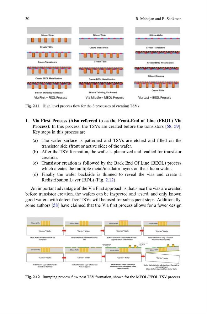
Fig. 2.11 High level process flow for the 3 processes of creating TSVs
1. Via First Process (Also referred to as the Front-End of Line (FEOL) Via
Process): In this process, the TSVs are created before the transistors [58, 59].
Key steps in this process are
(a) The wafer surface is patterned and TSVs are etched and filled on the
transistor side (front or active side) of the wafer.
(b) After the TSV formation, the wafer is planarized and readied for transistor
creation.
(c) Transistor creation is followed by the Back End Of Line (BEOL) process
which creates the multiple metal/insulator layers on the silicon wafer.
(d) Finally the wafer backside is thinned to reveal the vias and create a
Redistribution Layer (RDL) (Fig. 2.12).
An important advantage of the Via First approach is that since the vias are created
before transistor creation, the wafers can be inspected and tested, and only known
good wafers with defect-free TSVs will be used for subsequent steps. Additionally,
some authors [58] have claimed that the Via first process allows for a fewer design
Fig. 2.12 Bumping process flow post TSV formation, shown for the MEOL/FEOL TSV process
R. Mahajan and B. Sankman
Fig. 2.11 High level process flow for the 3 processes of creating TSVs
1. Via First Process (Also referred to as the Front-End of Line (FEOL) Via
Process): In this process, the TSVs are created before the transistors [58, 59].
Key steps in this process are
(a) The wafer surface is patterned and TSVs are etched and filled on the
transistor side (front or active side) of the wafer.
(b) After the TSV formation, the wafer is planarized and readied for transistor
creation.
(c) Transistor creation is followed by the Back End Of Line (BEOL) process
which creates the multiple metal/insulator layers on the silicon wafer.
(d) Finally the wafer backside is thinned to reveal the vias and create a
Redistribution Layer (RDL) (Fig. 2.12).
An important advantage of the Via First approach is that since the vias are created
before transistor creation, the wafers can be inspected and tested, and only known
good wafers with defect-free TSVs will be used for subsequent steps. Additionally,
some authors [58] have claimed that the Via first process allows for a fewer design
Fig. 2.12 Bumping process flow post TSV formation, shown for the MEOL/FEOL TSV process