

2 3D Packaging Architectures and Assembly Process Design
29
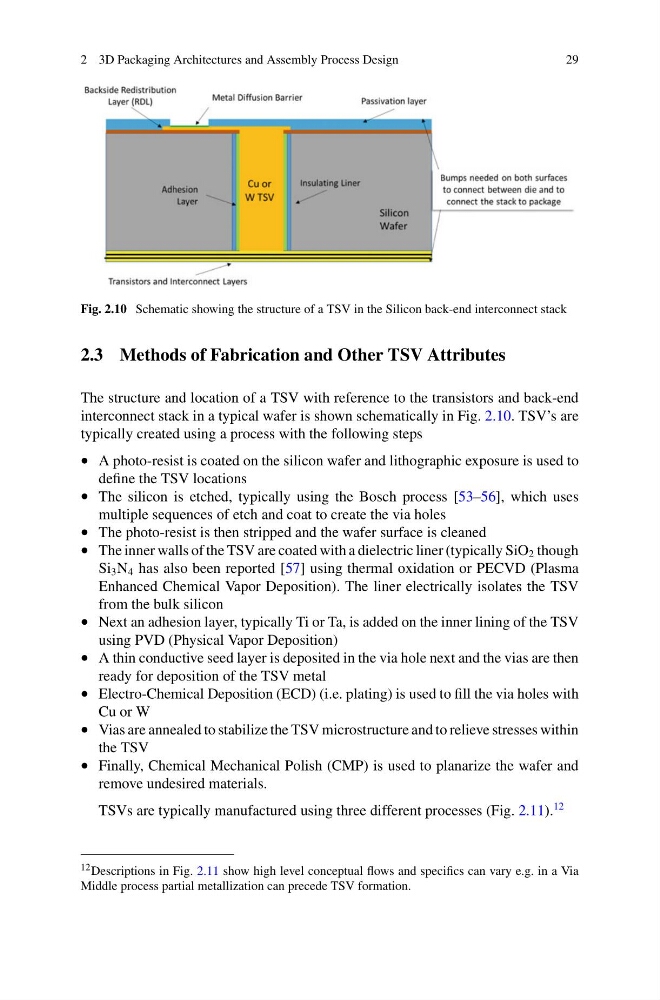
Fig. 2.10 Schematic showing the structure of a TSV in the Silicon back-end interconnect stack
2.3 Methods of Fabrication and Other TSV Attributes
The structure and location of a TSV with reference to the transistors and back-end
interconnect stack in a typical wafer is shown schematically in Fig. 2.10. TSV’s are
typically created using a process with the following steps
• A photo-resist is coated on the silicon wafer and lithographic exposure is used to
define the TSV locations
• The silicon is etched, typically using the Bosch process [53–56], which uses
multiple sequences of etch and coat to create the via holes
• The photo-resist is then stripped and the wafer surface is cleaned
• The inner walls of the TSV are coated with a dielectric liner (typically SiO 2 though
Si 3 N 4 has also been reported [57] using thermal oxidation or PECVD (Plasma
Enhanced Chemical Vapor Deposition). The liner electrically isolates the TSV
from the bulk silicon
• Next an adhesion layer, typically Ti or Ta, is added on the inner lining of the TSV
using PVD (Physical Vapor Deposition)
• A thin conductive seed layer is deposited in the via hole next and the vias are then
ready for deposition of the TSV metal
• Electro-Chemical Deposition (ECD) (i.e. plating) is used to fill the via holes with
Cu or W
• Vias are annealed to stabilize the TSV microstructure and to relieve stresses within
the TSV
• Finally, Chemical Mechanical Polish (CMP) is used to planarize the wafer and
remove undesired materials.
TSVs are typically manufactured using three different processes (Fig. 2.11).
12
12 Descriptions in Fig. 2.11 show high level conceptual flows and specifics can vary e.g. in a Via
Middle process partial metallization can precede TSV formation.
29
Fig. 2.10 Schematic showing the structure of a TSV in the Silicon back-end interconnect stack
2.3 Methods of Fabrication and Other TSV Attributes
The structure and location of a TSV with reference to the transistors and back-end
interconnect stack in a typical wafer is shown schematically in Fig. 2.10. TSV’s are
typically created using a process with the following steps
• A photo-resist is coated on the silicon wafer and lithographic exposure is used to
define the TSV locations
• The silicon is etched, typically using the Bosch process [53–56], which uses
multiple sequences of etch and coat to create the via holes
• The photo-resist is then stripped and the wafer surface is cleaned
• The inner walls of the TSV are coated with a dielectric liner (typically SiO 2 though
Si 3 N 4 has also been reported [57] using thermal oxidation or PECVD (Plasma
Enhanced Chemical Vapor Deposition). The liner electrically isolates the TSV
from the bulk silicon
• Next an adhesion layer, typically Ti or Ta, is added on the inner lining of the TSV
using PVD (Physical Vapor Deposition)
• A thin conductive seed layer is deposited in the via hole next and the vias are then
ready for deposition of the TSV metal
• Electro-Chemical Deposition (ECD) (i.e. plating) is used to fill the via holes with
Cu or W
• Vias are annealed to stabilize the TSV microstructure and to relieve stresses within
the TSV
• Finally, Chemical Mechanical Polish (CMP) is used to planarize the wafer and
remove undesired materials.
TSVs are typically manufactured using three different processes (Fig. 2.11).
12
12 Descriptions in Fig. 2.11 show high level conceptual flows and specifics can vary e.g. in a Via
Middle process partial metallization can precede TSV formation.