

28
R. Mahajan and B. Sankman
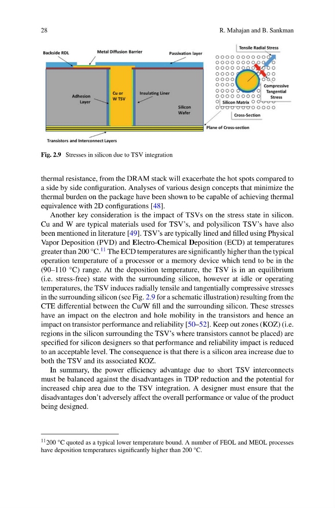
Fig. 2.9 Stresses in silicon due to TSV integration
thermal resistance, from the DRAM stack will exacerbate the hot spots compared to
a side by side configuration. Analyses of various design concepts that minimize the
thermal burden on the package have been shown to be capable of achieving thermal
equivalence with 2D configurations [48].
Another key consideration is the impact of TSVs on the stress state in silicon.
Cu and W are typical materials used for TSV’s, and polysilicon TSV’s have also
been mentioned in literature [49]. TSV’s are typically lined and filled using Physical
Vapor Deposition (PVD) and Electro-Chemical Deposition (ECD) at temperatures
greater than 200 °C.
11 The ECD temperatures are significantly higher than the typical
operation temperature of a processor or a memory device which tend to be in the
(90–110 °C) range. At the deposition temperature, the TSV is in an equilibrium
(i.e. stress-free) state with the surrounding silicon, however at idle or operating
temperatures, the TSV induces radially tensile and tangentially compressive stresses
in the surrounding silicon (see Fig. 2.9 for a schematic illustration) resulting from the
CTE differential between the Cu/W fill and the surrounding silicon. These stresses
have an impact on the electron and hole mobility in the transistors and hence an
impact on transistor performance and reliability [50–52]. Keep out zones (KOZ) (i.e.
regions in the silicon surrounding the TSV’s where transistors cannot be placed) are
specified for silicon designers so that performance and reliability impact is reduced
to an acceptable level. The consequence is that there is a silicon area increase due to
both the TSV and its associated KOZ.
In summary, the power efficiency advantage due to short TSV interconnects
must be balanced against the disadvantages in TDP reduction and the potential for
increased chip area due to the TSV integration. A designer must ensure that the
disadvantages don’t adversely affect the overall performance or value of the product
being designed.
11 200 °C quoted as a typical lower temperature bound. A number of FEOL and MEOL processes
have deposition temperatures significantly higher than 200 °C.
R. Mahajan and B. Sankman
Fig. 2.9 Stresses in silicon due to TSV integration
thermal resistance, from the DRAM stack will exacerbate the hot spots compared to
a side by side configuration. Analyses of various design concepts that minimize the
thermal burden on the package have been shown to be capable of achieving thermal
equivalence with 2D configurations [48].
Another key consideration is the impact of TSVs on the stress state in silicon.
Cu and W are typical materials used for TSV’s, and polysilicon TSV’s have also
been mentioned in literature [49]. TSV’s are typically lined and filled using Physical
Vapor Deposition (PVD) and Electro-Chemical Deposition (ECD) at temperatures
greater than 200 °C.
11 The ECD temperatures are significantly higher than the typical
operation temperature of a processor or a memory device which tend to be in the
(90–110 °C) range. At the deposition temperature, the TSV is in an equilibrium
(i.e. stress-free) state with the surrounding silicon, however at idle or operating
temperatures, the TSV induces radially tensile and tangentially compressive stresses
in the surrounding silicon (see Fig. 2.9 for a schematic illustration) resulting from the
CTE differential between the Cu/W fill and the surrounding silicon. These stresses
have an impact on the electron and hole mobility in the transistors and hence an
impact on transistor performance and reliability [50–52]. Keep out zones (KOZ) (i.e.
regions in the silicon surrounding the TSV’s where transistors cannot be placed) are
specified for silicon designers so that performance and reliability impact is reduced
to an acceptable level. The consequence is that there is a silicon area increase due to
both the TSV and its associated KOZ.
In summary, the power efficiency advantage due to short TSV interconnects
must be balanced against the disadvantages in TDP reduction and the potential for
increased chip area due to the TSV integration. A designer must ensure that the
disadvantages don’t adversely affect the overall performance or value of the product
being designed.
11 200 °C quoted as a typical lower temperature bound. A number of FEOL and MEOL processes
have deposition temperatures significantly higher than 200 °C.