

452
L. Chen et al.
smaller the gap is the stronger constraints that the die cap applies to the die, but the
higher risk the failure between the die and the die cap becomes.
Die cap thickness is the third major design parameter, and a proper thickness
may vary with different size of flip chip packages. For demonstration, a large size, a
medium size and a small size of packages are considered in the FEA simulation. The
large package is the same as the test vehicle, i.e., substrate size is 45 mm × 45 mm,
die size and thickness are 23 mm × 23 mm and 0.78 mm. The substrate has eight
metal layers and 0.8 mm thickness of core. The CTE and Young’s modulus of the
core are 11.3 ppm/°C and 32GPa. For the medium sized package, its substrate size
is 30 mm × 30 mm, die size and thickness are 17 mm × 17 mm and 0.3 mm. For
the small package, its substrate size is 20 mm × 20 mm, die size and thickness are
10 mm × 10 mm and 0.1 mm. The substrate of the medium sized package has six
metal layers and 0.4 mm thickness of core. The substrate of the small package has
six metal layers and 0.15 mm thickness of core. The core materials of the medium
and small packages are the same as the big package.
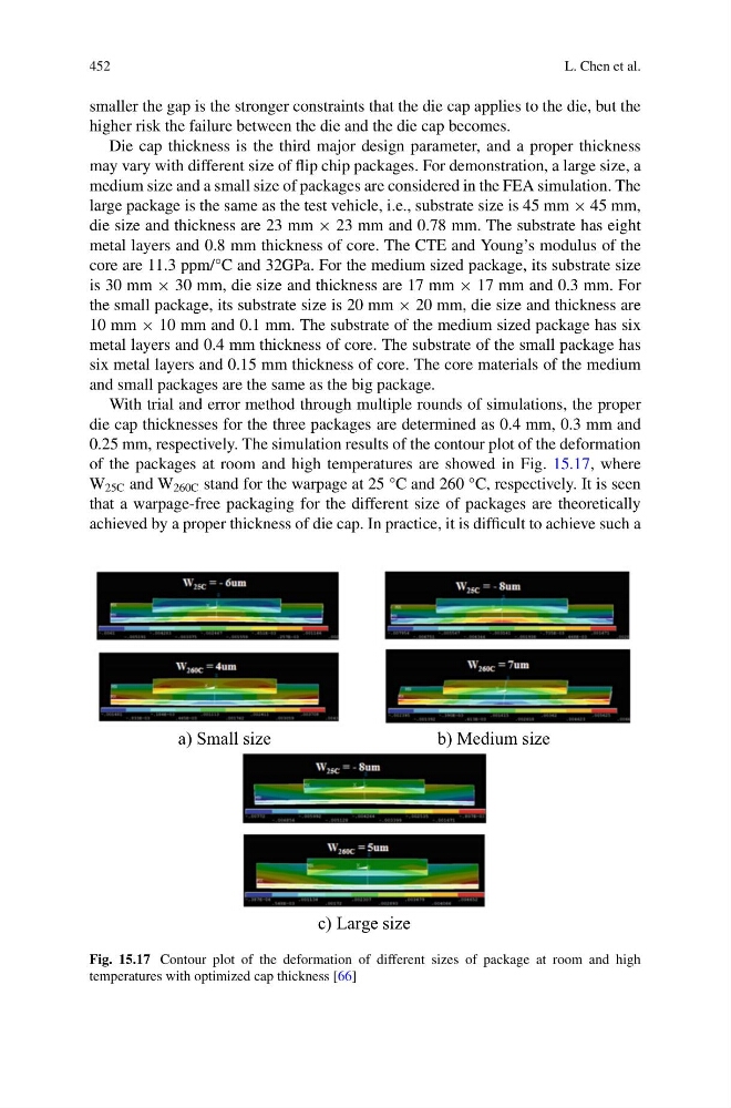
With trial and error method through multiple rounds of simulations, the proper
die cap thicknesses for the three packages are determined as 0.4 mm, 0.3 mm and
0.25 mm, respectively. The simulation results of the contour plot of the deformation
of the packages at room and high temperatures are showed in Fig. 15.17, where
W 25C and W 260C stand for the warpage at 25 °C and 260 °C, respectively. It is seen
that a warpage-free packaging for the different size of packages are theoretically
achieved by a proper thickness of die cap. In practice, it is difficult to achieve such a
a) Small size
b) Medium size
c) Large size
Fig. 15.17 Contour plot of the deformation of different sizes of package at room and high
temperatures with optimized cap thickness [66]
L. Chen et al.
smaller the gap is the stronger constraints that the die cap applies to the die, but the
higher risk the failure between the die and the die cap becomes.
Die cap thickness is the third major design parameter, and a proper thickness
may vary with different size of flip chip packages. For demonstration, a large size, a
medium size and a small size of packages are considered in the FEA simulation. The
large package is the same as the test vehicle, i.e., substrate size is 45 mm × 45 mm,
die size and thickness are 23 mm × 23 mm and 0.78 mm. The substrate has eight
metal layers and 0.8 mm thickness of core. The CTE and Young’s modulus of the
core are 11.3 ppm/°C and 32GPa. For the medium sized package, its substrate size
is 30 mm × 30 mm, die size and thickness are 17 mm × 17 mm and 0.3 mm. For
the small package, its substrate size is 20 mm × 20 mm, die size and thickness are
10 mm × 10 mm and 0.1 mm. The substrate of the medium sized package has six
metal layers and 0.4 mm thickness of core. The substrate of the small package has
six metal layers and 0.15 mm thickness of core. The core materials of the medium
and small packages are the same as the big package.
With trial and error method through multiple rounds of simulations, the proper
die cap thicknesses for the three packages are determined as 0.4 mm, 0.3 mm and
0.25 mm, respectively. The simulation results of the contour plot of the deformation
of the packages at room and high temperatures are showed in Fig. 15.17, where
W 25C and W 260C stand for the warpage at 25 °C and 260 °C, respectively. It is seen
that a warpage-free packaging for the different size of packages are theoretically
achieved by a proper thickness of die cap. In practice, it is difficult to achieve such a
a) Small size
b) Medium size
c) Large size
Fig. 15.17 Contour plot of the deformation of different sizes of package at room and high
temperatures with optimized cap thickness [66]