

450
L. Chen et al.
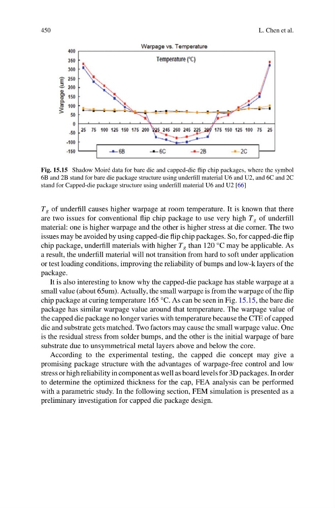
Fig. 15.15 Shadow Moiré data for bare die and capped-die flip chip packages, where the symbol
6B and 2B stand for bare die package structure using underfill material U6 and U2, and 6C and 2C
stand for Capped-die package structure using underfill material U6 and U2 [66]
T g of underfill causes higher warpage at room temperature. It is known that there
are two issues for conventional flip chip package to use very high T g of underfill
material: one is higher warpage and the other is higher stress at die corner. The two
issues may be avoided by using capped-die flip chip packages. So, for capped-die flip
chip package, underfill materials with higher T g than 120 °C may be applicable. As
a result, the underfill material will not transition from hard to soft under application
or test loading conditions, improving the reliability of bumps and low-k layers of the
package.
It is also interesting to know why the capped-die package has stable warpage at a
small value (about 65um). Actually, the small warpage is from the warpage of the flip
chip package at curing temperature 165 °C. As can be seen in Fig. 15.15, the bare die
package has similar warpage value around that temperature. The warpage value of
the capped die package no longer varies with temperature because the CTE of capped
die and substrate gets matched. Two factors may cause the small warpage value. One
is the residual stress from solder bumps, and the other is the initial warpage of bare
substrate due to unsymmetrical metal layers above and below the core.
According to the experimental testing, the capped die concept may give a
promising package structure with the advantages of warpage-free control and low
stress or high reliability in component as well as board levels for 3D packages. In order
to determine the optimized thickness for the cap, FEA analysis can be performed
with a parametric study. In the following section, FEM simulation is presented as a
preliminary investigation for capped die package design.
L. Chen et al.
Fig. 15.15 Shadow Moiré data for bare die and capped-die flip chip packages, where the symbol
6B and 2B stand for bare die package structure using underfill material U6 and U2, and 6C and 2C
stand for Capped-die package structure using underfill material U6 and U2 [66]
T g of underfill causes higher warpage at room temperature. It is known that there
are two issues for conventional flip chip package to use very high T g of underfill
material: one is higher warpage and the other is higher stress at die corner. The two
issues may be avoided by using capped-die flip chip packages. So, for capped-die flip
chip package, underfill materials with higher T g than 120 °C may be applicable. As
a result, the underfill material will not transition from hard to soft under application
or test loading conditions, improving the reliability of bumps and low-k layers of the
package.
It is also interesting to know why the capped-die package has stable warpage at a
small value (about 65um). Actually, the small warpage is from the warpage of the flip
chip package at curing temperature 165 °C. As can be seen in Fig. 15.15, the bare die
package has similar warpage value around that temperature. The warpage value of
the capped die package no longer varies with temperature because the CTE of capped
die and substrate gets matched. Two factors may cause the small warpage value. One
is the residual stress from solder bumps, and the other is the initial warpage of bare
substrate due to unsymmetrical metal layers above and below the core.
According to the experimental testing, the capped die concept may give a
promising package structure with the advantages of warpage-free control and low
stress or high reliability in component as well as board levels for 3D packages. In order
to determine the optimized thickness for the cap, FEA analysis can be performed
with a parametric study. In the following section, FEM simulation is presented as a
preliminary investigation for capped die package design.