

438
L. Chen et al.
Some distinct features of the curvature-temperature behavior of TSV structures as
seen in Fig. 15.4 are: stress relaxation during heating; linear curvature-temperature
relation during cooling; and absence of hysteresis loops. The stress relaxation
observed in the heating portion of each test is correlated to Cu grain growth in
the via, which is measured by electron backscatter diffraction (EBSD) (Fig. 15.4b).
A decrease of additive elements (Cl
− , F
− , S
− , and CN
− ) is found to accompany
grain growth as obtained by time-of-flight secondary ion mass spectroscopy (TOFSIMS) [39]. The linear cooling curvature observed in the experiment can be directly
correlated to the triaxial stress state (as shown in Fig. 15.2) obtained by FEA, as
the Cu via would remain mostly elastic with localized plasticity. This is in sharp
contrast with electroplated Cu thin films which have bi-axial stress state and show
hysteresis loops during thermal cycling [40]. The temperature at which the cooling
curvature crosses zero gives the reference temperature at which the average stress in
the TSVs is zero. With increased thermal cycling temperature, the amount of stress
relaxation increases during heating. This leads to higher stress-free temperatures and
accumulation of residual stress at room temperature after each thermal cycle.
Micro-Raman spectroscopy measures the near-surface stress in Si around the TSV
and complements the measurement by wafer curvature method. TSV specimen as
shown in Fig. 15.3 is used for the micro-Raman measurement [35]. Two specimens,
referred to as A and B, are subjected to different thermal treatment and their stressfree temperatures are determined to be T
A
re f = 100
◦ C and T
B
re f = 300
◦ C, from
wafer curvature measurement. The micro-Raman measurement is performed using
[001] backscattering configuration, and the signals are collected by scanning the
laser across two neighboring vias along the [110] direction in each sample.
In the test configuration, longitudinal Raman frequency shift, ω 3 , is measured
and can be correlated to the sum of the in-plane normal stresses, σ r + σ θ , through
Eq. (15.1) [42, 43]:
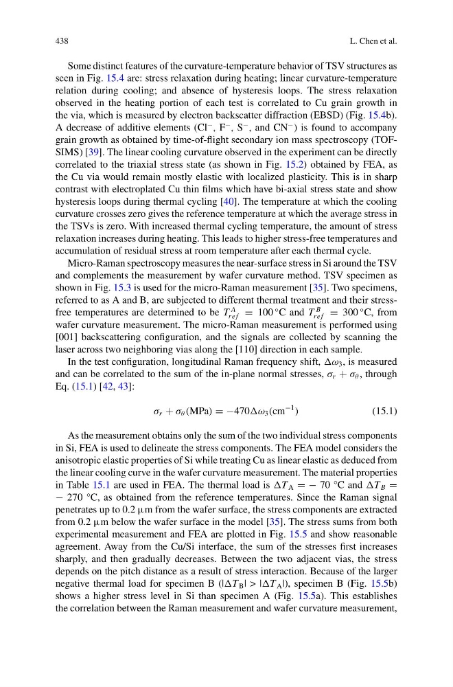
σ r + σ θ (MPa) = −470ω 3 (cm
−1
)
(15.1)
As the measurement obtains only the sum of the two individual stress components
in Si, FEA is used to delineate the stress components. The FEA model considers the
anisotropic elastic properties of Si while treating Cu as linear elastic as deduced from
the linear cooling curve in the wafer curvature measurement. The material properties
in Table 15.1 are used in FEA. The thermal load is T A = − 70 °C and T B =
− 270 °C, as obtained from the reference temperatures. Since the Raman signal
penetrates up to 0.2 μm from the wafer surface, the stress components are extracted
from 0.2 μm below the wafer surface in the model [35]. The stress sums from both
experimental measurement and FEA are plotted in Fig. 15.5 and show reasonable
agreement. Away from the Cu/Si interface, the sum of the stresses first increases
sharply, and then gradually decreases. Between the two adjacent vias, the stress
depends on the pitch distance as a result of stress interaction. Because of the larger
negative thermal load for specimen B (|T B | > |T A |), specimen B (Fig. 15.5b)
shows a higher stress level in Si than specimen A (Fig. 15.5a). This establishes
the correlation between the Raman measurement and wafer curvature measurement,
L. Chen et al.
Some distinct features of the curvature-temperature behavior of TSV structures as
seen in Fig. 15.4 are: stress relaxation during heating; linear curvature-temperature
relation during cooling; and absence of hysteresis loops. The stress relaxation
observed in the heating portion of each test is correlated to Cu grain growth in
the via, which is measured by electron backscatter diffraction (EBSD) (Fig. 15.4b).
A decrease of additive elements (Cl
− , F
− , S
− , and CN
− ) is found to accompany
grain growth as obtained by time-of-flight secondary ion mass spectroscopy (TOFSIMS) [39]. The linear cooling curvature observed in the experiment can be directly
correlated to the triaxial stress state (as shown in Fig. 15.2) obtained by FEA, as
the Cu via would remain mostly elastic with localized plasticity. This is in sharp
contrast with electroplated Cu thin films which have bi-axial stress state and show
hysteresis loops during thermal cycling [40]. The temperature at which the cooling
curvature crosses zero gives the reference temperature at which the average stress in
the TSVs is zero. With increased thermal cycling temperature, the amount of stress
relaxation increases during heating. This leads to higher stress-free temperatures and
accumulation of residual stress at room temperature after each thermal cycle.
Micro-Raman spectroscopy measures the near-surface stress in Si around the TSV
and complements the measurement by wafer curvature method. TSV specimen as
shown in Fig. 15.3 is used for the micro-Raman measurement [35]. Two specimens,
referred to as A and B, are subjected to different thermal treatment and their stressfree temperatures are determined to be T
A
re f = 100
◦ C and T
B
re f = 300
◦ C, from
wafer curvature measurement. The micro-Raman measurement is performed using
[001] backscattering configuration, and the signals are collected by scanning the
laser across two neighboring vias along the [110] direction in each sample.
In the test configuration, longitudinal Raman frequency shift, ω 3 , is measured
and can be correlated to the sum of the in-plane normal stresses, σ r + σ θ , through
Eq. (15.1) [42, 43]:
σ r + σ θ (MPa) = −470ω 3 (cm
−1
)
(15.1)
As the measurement obtains only the sum of the two individual stress components
in Si, FEA is used to delineate the stress components. The FEA model considers the
anisotropic elastic properties of Si while treating Cu as linear elastic as deduced from
the linear cooling curve in the wafer curvature measurement. The material properties
in Table 15.1 are used in FEA. The thermal load is T A = − 70 °C and T B =
− 270 °C, as obtained from the reference temperatures. Since the Raman signal
penetrates up to 0.2 μm from the wafer surface, the stress components are extracted
from 0.2 μm below the wafer surface in the model [35]. The stress sums from both
experimental measurement and FEA are plotted in Fig. 15.5 and show reasonable
agreement. Away from the Cu/Si interface, the sum of the stresses first increases
sharply, and then gradually decreases. Between the two adjacent vias, the stress
depends on the pitch distance as a result of stress interaction. Because of the larger
negative thermal load for specimen B (|T B | > |T A |), specimen B (Fig. 15.5b)
shows a higher stress level in Si than specimen A (Fig. 15.5a). This establishes
the correlation between the Raman measurement and wafer curvature measurement,