

15 Die and Package Level Thermal and Thermal/Moisture Stresses …
437
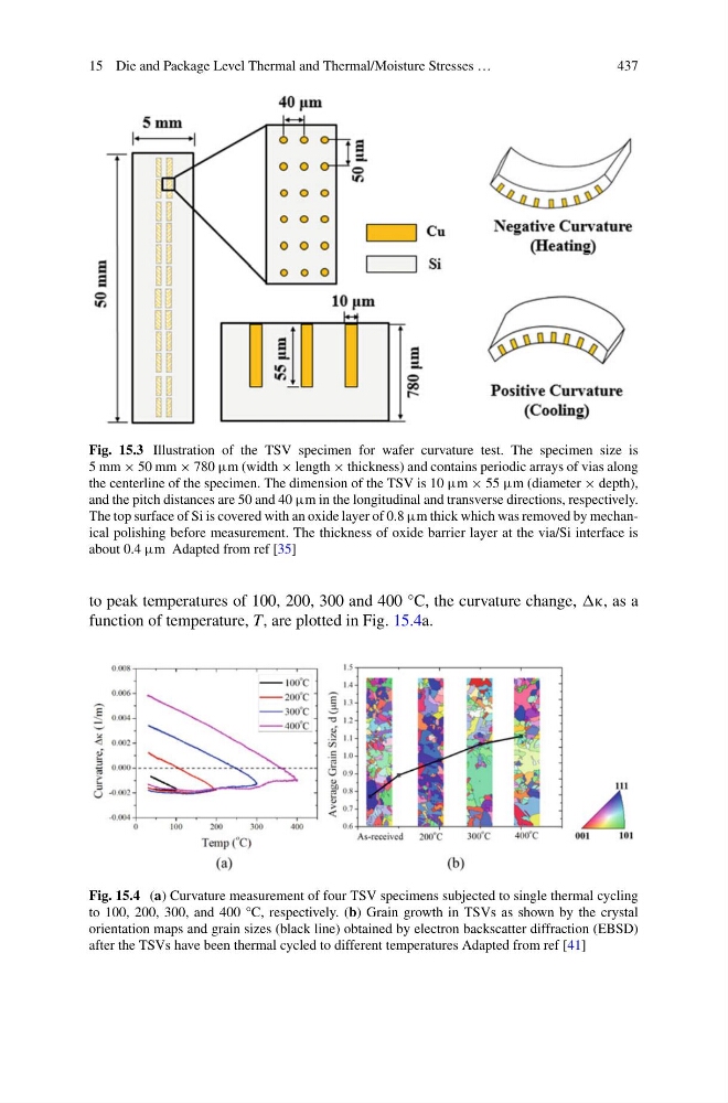
Fig. 15.3 Illustration of the TSV specimen for wafer curvature test. The specimen size is
5 mm × 50 mm × 780 μm (width × length × thickness) and contains periodic arrays of vias along
the centerline of the specimen. The dimension of the TSV is 10 μm × 55 μm (diameter × depth),
and the pitch distances are 50 and 40 μm in the longitudinal and transverse directions, respectively.
The top surface of Si is covered with an oxide layer of 0.8 μm thick which was removed by mechanical polishing before measurement. The thickness of oxide barrier layer at the via/Si interface is
about 0.4 μm Adapted from ref [35]
to peak temperatures of 100, 200, 300 and 400 °C, the curvature change, κ, as a
function of temperature, T, are plotted in Fig. 15.4a.
Fig. 15.4 (a) Curvature measurement of four TSV specimens subjected to single thermal cycling
to 100, 200, 300, and 400 °C, respectively. (b) Grain growth in TSVs as shown by the crystal
orientation maps and grain sizes (black line) obtained by electron backscatter diffraction (EBSD)
after the TSVs have been thermal cycled to different temperatures Adapted from ref [41]
437
Fig. 15.3 Illustration of the TSV specimen for wafer curvature test. The specimen size is
5 mm × 50 mm × 780 μm (width × length × thickness) and contains periodic arrays of vias along
the centerline of the specimen. The dimension of the TSV is 10 μm × 55 μm (diameter × depth),
and the pitch distances are 50 and 40 μm in the longitudinal and transverse directions, respectively.
The top surface of Si is covered with an oxide layer of 0.8 μm thick which was removed by mechanical polishing before measurement. The thickness of oxide barrier layer at the via/Si interface is
about 0.4 μm Adapted from ref [35]
to peak temperatures of 100, 200, 300 and 400 °C, the curvature change, κ, as a
function of temperature, T, are plotted in Fig. 15.4a.
Fig. 15.4 (a) Curvature measurement of four TSV specimens subjected to single thermal cycling
to 100, 200, 300, and 400 °C, respectively. (b) Grain growth in TSVs as shown by the crystal
orientation maps and grain sizes (black line) obtained by electron backscatter diffraction (EBSD)
after the TSVs have been thermal cycled to different temperatures Adapted from ref [41]