

436
L. Chen et al.
Table 15.1 Thermomechanical properties used in
finite element analysis
Material
CTE
(ppm/ o C)
Young’s Modulus
(GPa)
Poisson’s ratio
Cu
17
110
0.35
Si
2.3
130
0.28
Oxide
0.55
72
0.16
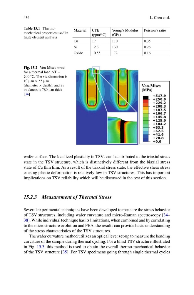
Fig. 15.2 Von-Mises stress
for a thermal load T =
200 °C. The via dimension is
10 μm × 55 μm
(diameter × depth), and Si
thickness is 780 μm thick
[34]
wafer surface. The localized plasticity in TSVs can be attributed to the triaxial stress
state in the TSV structure, which is distinctively different from the biaxial stress
state of Cu thin film. As a result of the triaxial stress state, the effective shear stress
causing plastic deformation is relatively low in TSV structures. This has important
implications on TSV reliability which will be discussed in the rest of this section.
15.2.3 Measurement of Thermal Stress
Several experimental techniques have been developed to measure the stress behavior
of TSV structures, including wafer curvature and micro-Raman spectroscopy [34–
38]. While individual technique has its limitations, when combined and by correlating
to the microstructure evolution and FEA, the results can provide basic understanding
of the stress characteristics of the TSV structures.
The wafer curvature method utilizes an optical lever set-up to measure the bending
curvature of the sample during thermal cycling. For a blind TSV structure illustrated
in Fig. 15.3, this method is used to obtain the overall thermo-mechanical behavior
of the TSV structure [35]. For TSV specimens going through single thermal cycles
L. Chen et al.
Table 15.1 Thermomechanical properties used in
finite element analysis
Material
CTE
(ppm/ o C)
Young’s Modulus
(GPa)
Poisson’s ratio
Cu
17
110
0.35
Si
2.3
130
0.28
Oxide
0.55
72
0.16
Fig. 15.2 Von-Mises stress
for a thermal load T =
200 °C. The via dimension is
10 μm × 55 μm
(diameter × depth), and Si
thickness is 780 μm thick
[34]
wafer surface. The localized plasticity in TSVs can be attributed to the triaxial stress
state in the TSV structure, which is distinctively different from the biaxial stress
state of Cu thin film. As a result of the triaxial stress state, the effective shear stress
causing plastic deformation is relatively low in TSV structures. This has important
implications on TSV reliability which will be discussed in the rest of this section.
15.2.3 Measurement of Thermal Stress
Several experimental techniques have been developed to measure the stress behavior
of TSV structures, including wafer curvature and micro-Raman spectroscopy [34–
38]. While individual technique has its limitations, when combined and by correlating
to the microstructure evolution and FEA, the results can provide basic understanding
of the stress characteristics of the TSV structures.
The wafer curvature method utilizes an optical lever set-up to measure the bending
curvature of the sample during thermal cycling. For a blind TSV structure illustrated
in Fig. 15.3, this method is used to obtain the overall thermo-mechanical behavior
of the TSV structure [35]. For TSV specimens going through single thermal cycles