

15 Die and Package Level Thermal and Thermal/Moisture Stresses …
435
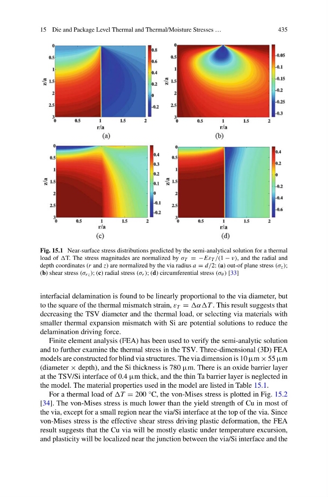
Fig. 15.1 Near-surface stress distributions predicted by the semi-analytical solution for a thermal
load of T. The stress magnitudes are normalized by σ T = −Eε T /(1 − ν), and the radial and
depth coordinates (r and z) are normalized by the via radius a = d/2: (a) out-of plane stress (σ z );
(b) shear stress (σ r z ); (c) radial stress (σ r ); (d) circumferential stress (σ θ ) [33]
interfacial delamination is found to be linearly proportional to the via diameter, but
to the square of the thermal mismatch strain, ε T = . This result suggests that
decreasing the TSV diameter and the thermal load, or selecting via materials with
smaller thermal expansion mismatch with Si are potential solutions to reduce the
delamination driving force.
Finite element analysis (FEA) has been used to verify the semi-analytic solution
and to further examine the thermal stress in the TSV. Three-dimensional (3D) FEA
models are constructed for blind via structures. The via dimension is 10 μm × 55 μm
(diameter × depth), and the Si thickness is 780 μm. There is an oxide barrier layer
at the TSV/Si interface of 0.4 μm thick, and the thin Ta barrier layer is neglected in
the model. The material properties used in the model are listed in Table 15.1.
For a thermal load of T = 200 °C, the von-Mises stress is plotted in Fig. 15.2
[34]. The von-Mises stress is much lower than the yield strength of Cu in most of
the via, except for a small region near the via/Si interface at the top of the via. Since
von-Mises stress is the effective shear stress driving plastic deformation, the FEA
result suggests that the Cu via will be mostly elastic under temperature excursion,
and plasticity will be localized near the junction between the via/Si interface and the
435
Fig. 15.1 Near-surface stress distributions predicted by the semi-analytical solution for a thermal
load of T. The stress magnitudes are normalized by σ T = −Eε T /(1 − ν), and the radial and
depth coordinates (r and z) are normalized by the via radius a = d/2: (a) out-of plane stress (σ z );
(b) shear stress (σ r z ); (c) radial stress (σ r ); (d) circumferential stress (σ θ ) [33]
interfacial delamination is found to be linearly proportional to the via diameter, but
to the square of the thermal mismatch strain, ε T = . This result suggests that
decreasing the TSV diameter and the thermal load, or selecting via materials with
smaller thermal expansion mismatch with Si are potential solutions to reduce the
delamination driving force.
Finite element analysis (FEA) has been used to verify the semi-analytic solution
and to further examine the thermal stress in the TSV. Three-dimensional (3D) FEA
models are constructed for blind via structures. The via dimension is 10 μm × 55 μm
(diameter × depth), and the Si thickness is 780 μm. There is an oxide barrier layer
at the TSV/Si interface of 0.4 μm thick, and the thin Ta barrier layer is neglected in
the model. The material properties used in the model are listed in Table 15.1.
For a thermal load of T = 200 °C, the von-Mises stress is plotted in Fig. 15.2
[34]. The von-Mises stress is much lower than the yield strength of Cu in most of
the via, except for a small region near the via/Si interface at the top of the via. Since
von-Mises stress is the effective shear stress driving plastic deformation, the FEA
result suggests that the Cu via will be mostly elastic under temperature excursion,
and plasticity will be localized near the junction between the via/Si interface and the