

15 Die and Package Level Thermal and Thermal/Moisture Stresses …
439
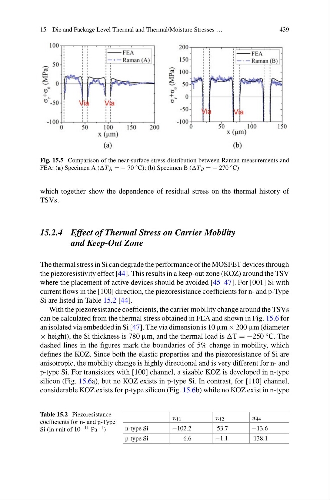
Fig. 15.5 Comparison of the near-surface stress distribution between Raman measurements and
FEA: (a) Specimen A (T A = − 70 °C); (b) Specimen B (T B = − 270 °C)
which together show the dependence of residual stress on the thermal history of
TSVs.
15.2.4 Effect of Thermal Stress on Carrier Mobility
and Keep-Out Zone
The thermal stress in Si can degrade the performance of the MOSFET devices through
the piezoresistivity effect [44]. This results in a keep-out zone (KOZ) around the TSV
where the placement of active devices should be avoided [45–47]. For [001] Si with
current flows in the [100] direction, the piezoresistance coefficients for n- and p-Type
Si are listed in Table 15.2 [44].
With the piezoresistance coefficients, the carrier mobility change around the TSVs
can be calculated from the thermal stress obtained in FEA and shown in Fig. 15.6 for
an isolated via embedded in Si [47]. The via dimension is 10 μm × 200 μm (diameter
× height), the Si thickness is 780 μm, and the thermal load is T = −250 °C. The
dashed lines in the figures mark the boundaries of 5% change in mobility, which
defines the KOZ. Since both the elastic properties and the piezoresistance of Si are
anisotropic, the mobility change is highly directional and is very different for n- and
p-type Si. For transistors with [100] channel, a sizable KOZ is developed in n-type
silicon (Fig. 15.6a), but no KOZ exists in p-type Si. In contrast, for [110] channel,
considerable KOZ exists for p-type silicon (Fig. 15.6b) while no KOZ exist in n-type
Table 15.2 Piezoresistance
coefficients for n- and p-Type
Si (in unit of 10 −11 Pa −1 )
π 11
π 12
π 44
n-type Si
−102.2
53.7
−13.6
p-type Si
6.6
−1.1
138.1
439
Fig. 15.5 Comparison of the near-surface stress distribution between Raman measurements and
FEA: (a) Specimen A (T A = − 70 °C); (b) Specimen B (T B = − 270 °C)
which together show the dependence of residual stress on the thermal history of
TSVs.
15.2.4 Effect of Thermal Stress on Carrier Mobility
and Keep-Out Zone
The thermal stress in Si can degrade the performance of the MOSFET devices through
the piezoresistivity effect [44]. This results in a keep-out zone (KOZ) around the TSV
where the placement of active devices should be avoided [45–47]. For [001] Si with
current flows in the [100] direction, the piezoresistance coefficients for n- and p-Type
Si are listed in Table 15.2 [44].
With the piezoresistance coefficients, the carrier mobility change around the TSVs
can be calculated from the thermal stress obtained in FEA and shown in Fig. 15.6 for
an isolated via embedded in Si [47]. The via dimension is 10 μm × 200 μm (diameter
× height), the Si thickness is 780 μm, and the thermal load is T = −250 °C. The
dashed lines in the figures mark the boundaries of 5% change in mobility, which
defines the KOZ. Since both the elastic properties and the piezoresistance of Si are
anisotropic, the mobility change is highly directional and is very different for n- and
p-type Si. For transistors with [100] channel, a sizable KOZ is developed in n-type
silicon (Fig. 15.6a), but no KOZ exists in p-type Si. In contrast, for [110] channel,
considerable KOZ exists for p-type silicon (Fig. 15.6b) while no KOZ exist in n-type
Table 15.2 Piezoresistance
coefficients for n- and p-Type
Si (in unit of 10 −11 Pa −1 )
π 11
π 12
π 44
n-type Si
−102.2
53.7
−13.6
p-type Si
6.6
−1.1
138.1