

426
S. Shi et al.
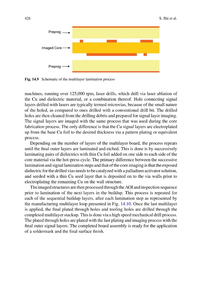
Fig. 14.9 Schematic of the multilayer lamination process
machines, running over 125,000 rpm, laser drills, which drill via laser ablation of
the Cu and dielectric material, or a combination thereof. Hole connecting signal
layers drilled with lasers are typically termed microvias, because of the small nature
of the holed, as compared to ones drilled with a conventional drill bit. The drilled
holes are then cleaned from the drilling debris and prepared for signal layer imaging.
The signal layers are imaged with the same process that was used during the core
fabrication process. The only difference is that the Cu signal layers are electroplated
up from the base Cu foil to the desired thickness via a pattern plating or equivalent
process.
Depending on the number of layers of the multilayer board, the process repeats
until the final outer layers are laminated and etched. This is done is by successively
laminating pairs of dielectrics with thin Cu foil added on one side to each side of the
core material via the hot-press cycle. The primary difference between the successive
lamination and signal lamination steps and that of the core imaging is that the exposed
dielectric for the drilled vias needs to be catalyzed with a palladium activator solution,
and seeded with a thin Cu seed layer that is deposited on to the via walls prior to
electroplating the remaining Cu on the wall structure.
The imaged structures are then processed through the AOI and inspection sequence
prior to lamination of the next layers in the buildup. This process is repeated for
each of the sequential buildup layers, after each lamination step as represented by
the manufacturing multilayer loop presented in Fig. 14.10. Once the last multilayer
is applied, the final plated through holes and tooling holes are drilled through the
completed multilayer stackup. This is done via a high speed mechanical drill process.
The plated through holes are plated with the last plating and imaging process with the
final outer signal layers. The completed board assembly is ready for the application
of a soldermask and the final surface finish.
S. Shi et al.
Fig. 14.9 Schematic of the multilayer lamination process
machines, running over 125,000 rpm, laser drills, which drill via laser ablation of
the Cu and dielectric material, or a combination thereof. Hole connecting signal
layers drilled with lasers are typically termed microvias, because of the small nature
of the holed, as compared to ones drilled with a conventional drill bit. The drilled
holes are then cleaned from the drilling debris and prepared for signal layer imaging.
The signal layers are imaged with the same process that was used during the core
fabrication process. The only difference is that the Cu signal layers are electroplated
up from the base Cu foil to the desired thickness via a pattern plating or equivalent
process.
Depending on the number of layers of the multilayer board, the process repeats
until the final outer layers are laminated and etched. This is done is by successively
laminating pairs of dielectrics with thin Cu foil added on one side to each side of the
core material via the hot-press cycle. The primary difference between the successive
lamination and signal lamination steps and that of the core imaging is that the exposed
dielectric for the drilled vias needs to be catalyzed with a palladium activator solution,
and seeded with a thin Cu seed layer that is deposited on to the via walls prior to
electroplating the remaining Cu on the wall structure.
The imaged structures are then processed through the AOI and inspection sequence
prior to lamination of the next layers in the buildup. This process is repeated for
each of the sequential buildup layers, after each lamination step as represented by
the manufacturing multilayer loop presented in Fig. 14.10. Once the last multilayer
is applied, the final plated through holes and tooling holes are drilled through the
completed multilayer stackup. This is done via a high speed mechanical drill process.
The plated through holes are plated with the last plating and imaging process with the
final outer signal layers. The completed board assembly is ready for the application
of a soldermask and the final surface finish.