

22
R. Mahajan and B. Sankman
c
d
(i)
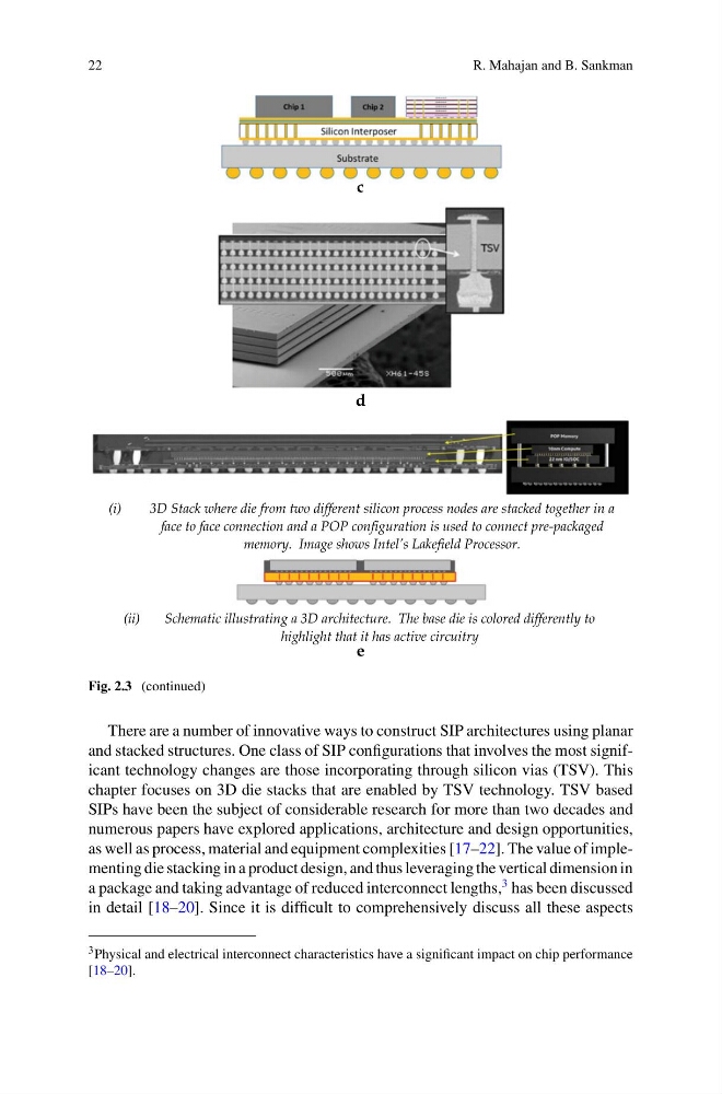
3D Stack where die from two different silicon process nodes are stacked together in a
face to face connection and a POP configuration is used to connect pre-packaged
memory. Image shows Intel’s Lakefield Processor.
(ii)
Schematic illustrating a 3D architecture. The base die is colored differently to
highlight that it has active circuitry
e
Fig. 2.3 (continued)
There are a number of innovative ways to construct SIP architectures using planar
and stacked structures. One class of SIP configurations that involves the most significant technology changes are those incorporating through silicon vias (TSV). This
chapter focuses on 3D die stacks that are enabled by TSV technology. TSV based
SIPs have been the subject of considerable research for more than two decades and
numerous papers have explored applications, architecture and design opportunities,
as well as process, material and equipment complexities [17–22]. The value of implementing die stacking in a product design, and thus leveraging the vertical dimension in
a package and taking advantage of reduced interconnect lengths,
3 has been discussed
in detail [18–20]. Since it is difficult to comprehensively discuss all these aspects
3 Physical and electrical interconnect characteristics have a significant impact on chip performance
[18–20].
R. Mahajan and B. Sankman
c
d
(i)
3D Stack where die from two different silicon process nodes are stacked together in a
face to face connection and a POP configuration is used to connect pre-packaged
memory. Image shows Intel’s Lakefield Processor.
(ii)
Schematic illustrating a 3D architecture. The base die is colored differently to
highlight that it has active circuitry
e
Fig. 2.3 (continued)
There are a number of innovative ways to construct SIP architectures using planar
and stacked structures. One class of SIP configurations that involves the most significant technology changes are those incorporating through silicon vias (TSV). This
chapter focuses on 3D die stacks that are enabled by TSV technology. TSV based
SIPs have been the subject of considerable research for more than two decades and
numerous papers have explored applications, architecture and design opportunities,
as well as process, material and equipment complexities [17–22]. The value of implementing die stacking in a product design, and thus leveraging the vertical dimension in
a package and taking advantage of reduced interconnect lengths,
3 has been discussed
in detail [18–20]. Since it is difficult to comprehensively discuss all these aspects
3 Physical and electrical interconnect characteristics have a significant impact on chip performance
[18–20].