

2 3D Packaging Architectures and Assembly Process Design
21
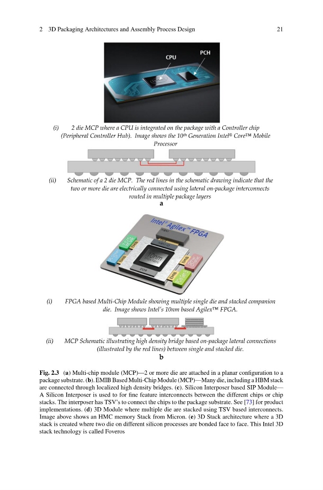
(ii)
Schematic of a 2 die MCP. The red lines in the schematic drawing indicate that the
two or more die are electrically connected using lateral on-package interconnects
routed in multiple package layers
a
(i)
2 die MCP where a CPU is integrated on the package with a Controller chip
(Peripheral Controller Hub). Image shows the 10 th Generation Intel ® Core™ Mobile
Processor
(i)
FPGA based Multi-Chip Module showing multiple single die and stacked companion
die. Image shows Intel’s 10nm based Agilex™ FPGA.
(ii)
MCP Schematic illustrating high density bridge based on-package lateral connections
(illustrated by the red lines) between single and stacked die.
b
Fig. 2.3 (a) Multi-chip module (MCP)—2 or more die are attached in a planar configuration to a
package substrate. (b). EMIB Based Multi-Chip Module (MCP)—Many die, including a HBM stack
are connected through localized high density bridges. (c). Silicon Interposer based SIP Module—
A Silicon Interposer is used to for fine feature interconnects between the different chips or chip
stacks. The interposer has TSV’s to connect the chips to the package substrate. See [73] for product
implementations. (d) 3D Module where multiple die are stacked using TSV based interconnects.
Image above shows an HMC memory Stack from Micron. (e) 3D Stack architecture where a 3D
stack is created where two die on different silicon processes are bonded face to face. This Intel 3D
stack technology is called Foveros
21
(ii)
Schematic of a 2 die MCP. The red lines in the schematic drawing indicate that the
two or more die are electrically connected using lateral on-package interconnects
routed in multiple package layers
a
(i)
2 die MCP where a CPU is integrated on the package with a Controller chip
(Peripheral Controller Hub). Image shows the 10 th Generation Intel ® Core™ Mobile
Processor
(i)
FPGA based Multi-Chip Module showing multiple single die and stacked companion
die. Image shows Intel’s 10nm based Agilex™ FPGA.
(ii)
MCP Schematic illustrating high density bridge based on-package lateral connections
(illustrated by the red lines) between single and stacked die.
b
Fig. 2.3 (a) Multi-chip module (MCP)—2 or more die are attached in a planar configuration to a
package substrate. (b). EMIB Based Multi-Chip Module (MCP)—Many die, including a HBM stack
are connected through localized high density bridges. (c). Silicon Interposer based SIP Module—
A Silicon Interposer is used to for fine feature interconnects between the different chips or chip
stacks. The interposer has TSV’s to connect the chips to the package substrate. See [73] for product
implementations. (d) 3D Module where multiple die are stacked using TSV based interconnects.
Image above shows an HMC memory Stack from Micron. (e) 3D Stack architecture where a 3D
stack is created where two die on different silicon processes are bonded face to face. This Intel 3D
stack technology is called Foveros