

12 Fundamentals of Electromigration in Interconnects of 3D Packaging
365
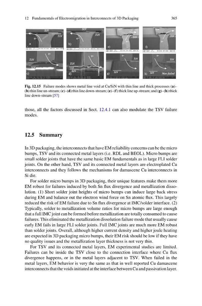
Fig. 12.15 Failure modes shows metal line void at Cu/SiN with thin line and thick processes (a)–
(b) thin line un-stream; (c)–(d) thin line down-stream; (e)–(f) thick line up-stream; and (g)–(h) thick
line down-stream [57]
those, all the factors discussed in Sect. 12.4.1 can also modulate the TSV failure
modes.
12.5 Summary
In 3D packaging, the interconnects that have EM reliability concerns can be the micro
bumps, TSV and its connected metal layers (i.e. RDL and BEOL). Micro bumps are
small solder joints that have the same basic EM fundamentals as in large FLI solder
joints. On the other hand, TSV and its connected metal layers are electroplated Cu
interconnects and they follows the mechanisms for damascene Cu interconnects in
Si die.
For solder micro bumps in 3D packaging, their unique features make them more
EM robust for failures induced by both Sn flux divergence and metallization dissolution. (1) Short solder joint heights of micro bumps can induce large back stress
during EM and balance out the electron wind force on Sn atomic flux. This largely
reduced the risk of EM failure due to Sn flux divergence at IMC/solder interface. (2)
Typically, solder to metallization volume ratios for micro bumps are large enough
that a full IMC joint can be formed before metallization are totally consumed to cause
failures. This eliminated the metallization dissolution failure mode that usually cause
early EM fails in large FLI solder joints. Full IMC joints are much more EM robust
than solder joints. Overall, although higher current density and higher joule heating
are expected in 3D packaging micro bumps, their EM risk should be low if they have
no quality issues and the metallization layer thickness is not very thin.
For TSV and its connected metal layers, EM experimental studies are limited.
Failures can be inside the TSV close to the connection interface where Cu flux
divergence happens, or in the metal layers adjacent to TSV. When failed in the
metal layers, EM behavior is very the same as that in well reported Cu damascene
interconnects that the voids initiated at the interface between Cu and passivation layer.
365
Fig. 12.15 Failure modes shows metal line void at Cu/SiN with thin line and thick processes (a)–
(b) thin line un-stream; (c)–(d) thin line down-stream; (e)–(f) thick line up-stream; and (g)–(h) thick
line down-stream [57]
those, all the factors discussed in Sect. 12.4.1 can also modulate the TSV failure
modes.
12.5 Summary
In 3D packaging, the interconnects that have EM reliability concerns can be the micro
bumps, TSV and its connected metal layers (i.e. RDL and BEOL). Micro bumps are
small solder joints that have the same basic EM fundamentals as in large FLI solder
joints. On the other hand, TSV and its connected metal layers are electroplated Cu
interconnects and they follows the mechanisms for damascene Cu interconnects in
Si die.
For solder micro bumps in 3D packaging, their unique features make them more
EM robust for failures induced by both Sn flux divergence and metallization dissolution. (1) Short solder joint heights of micro bumps can induce large back stress
during EM and balance out the electron wind force on Sn atomic flux. This largely
reduced the risk of EM failure due to Sn flux divergence at IMC/solder interface. (2)
Typically, solder to metallization volume ratios for micro bumps are large enough
that a full IMC joint can be formed before metallization are totally consumed to cause
failures. This eliminated the metallization dissolution failure mode that usually cause
early EM fails in large FLI solder joints. Full IMC joints are much more EM robust
than solder joints. Overall, although higher current density and higher joule heating
are expected in 3D packaging micro bumps, their EM risk should be low if they have
no quality issues and the metallization layer thickness is not very thin.
For TSV and its connected metal layers, EM experimental studies are limited.
Failures can be inside the TSV close to the connection interface where Cu flux
divergence happens, or in the metal layers adjacent to TSV. When failed in the
metal layers, EM behavior is very the same as that in well reported Cu damascene
interconnects that the voids initiated at the interface between Cu and passivation layer.