

12 Fundamentals of Electromigration in Interconnects of 3D Packaging
357
12.3.2 The Transformation of Full IMC Joint Under EM
Micro bump under EM has another unique behavior comparing with larger solder
joints. It typically has smaller solder to metallization volume ratio, which can form
a full IMC bump before the metallization is fully consumed. This is the reason that
metallization dissolution as discussed in Sect. 12.2.2 is not the key reported failure
mode in micro bumps.
The threshold volume ratio of metallization to solder to form full IMC instead of
induce metallization dissolution failure mode can be simply calculated based on the
IMC reaction equation. Take Cu/Sn reaction as an example, Cu 6 Sn 5 IMC is always
formed first with the dissolution of Cu under EM. It can be calculated that when Cu
to Sn volume ratio is larger than 0.52, a full Cu 6 Sn 5 IMC bump will be formed. In
other words, as long as the Cu height is longer than half of the solder height, a full
IMC joint will be formed before it failed as Cu dissolution.
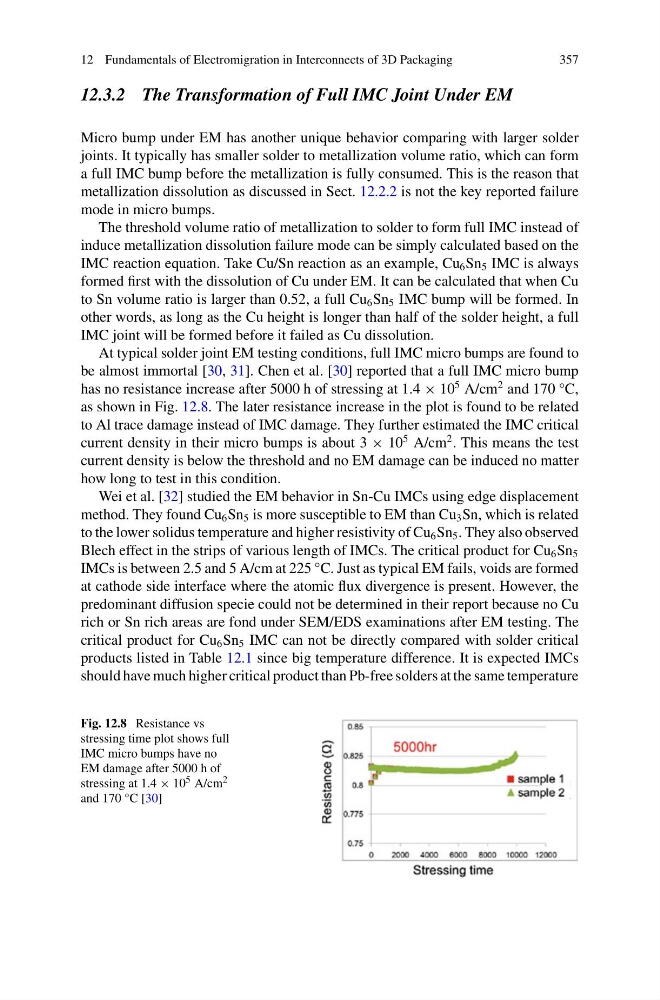
At typical solder joint EM testing conditions, full IMC micro bumps are found to
be almost immortal [30, 31]. Chen et al. [30] reported that a full IMC micro bump
has no resistance increase after 5000 h of stressing at 1.4 × 10
5 A/cm
2 and 170 °C,
as shown in Fig. 12.8. The later resistance increase in the plot is found to be related
to Al trace damage instead of IMC damage. They further estimated the IMC critical
current density in their micro bumps is about 3 × 10
5 A/cm
2 . This means the test
current density is below the threshold and no EM damage can be induced no matter
how long to test in this condition.
Wei et al. [32] studied the EM behavior in Sn-Cu IMCs using edge displacement
method. They found Cu 6 Sn 5 is more susceptible to EM than Cu 3 Sn, which is related
to the lower solidus temperature and higher resistivity of Cu 6 Sn 5 . They also observed
Blech effect in the strips of various length of IMCs. The critical product for Cu 6 Sn 5
IMCs is between 2.5 and 5 A/cm at 225 °C. Just as typical EM fails, voids are formed
at cathode side interface where the atomic flux divergence is present. However, the
predominant diffusion specie could not be determined in their report because no Cu
rich or Sn rich areas are fond under SEM/EDS examinations after EM testing. The
critical product for Cu 6 Sn 5 IMC can not be directly compared with solder critical
products listed in Table 12.1 since big temperature difference. It is expected IMCs
should have much higher critical product than Pb-free solders at the same temperature
Fig. 12.8 Resistance vs
stressing time plot shows full
IMC micro bumps have no
EM damage after 5000 h of
stressing at 1.4 × 10 5 A/cm 2
and 170 °C [30]
357
12.3.2 The Transformation of Full IMC Joint Under EM
Micro bump under EM has another unique behavior comparing with larger solder
joints. It typically has smaller solder to metallization volume ratio, which can form
a full IMC bump before the metallization is fully consumed. This is the reason that
metallization dissolution as discussed in Sect. 12.2.2 is not the key reported failure
mode in micro bumps.
The threshold volume ratio of metallization to solder to form full IMC instead of
induce metallization dissolution failure mode can be simply calculated based on the
IMC reaction equation. Take Cu/Sn reaction as an example, Cu 6 Sn 5 IMC is always
formed first with the dissolution of Cu under EM. It can be calculated that when Cu
to Sn volume ratio is larger than 0.52, a full Cu 6 Sn 5 IMC bump will be formed. In
other words, as long as the Cu height is longer than half of the solder height, a full
IMC joint will be formed before it failed as Cu dissolution.
At typical solder joint EM testing conditions, full IMC micro bumps are found to
be almost immortal [30, 31]. Chen et al. [30] reported that a full IMC micro bump
has no resistance increase after 5000 h of stressing at 1.4 × 10
5 A/cm
2 and 170 °C,
as shown in Fig. 12.8. The later resistance increase in the plot is found to be related
to Al trace damage instead of IMC damage. They further estimated the IMC critical
current density in their micro bumps is about 3 × 10
5 A/cm
2 . This means the test
current density is below the threshold and no EM damage can be induced no matter
how long to test in this condition.
Wei et al. [32] studied the EM behavior in Sn-Cu IMCs using edge displacement
method. They found Cu 6 Sn 5 is more susceptible to EM than Cu 3 Sn, which is related
to the lower solidus temperature and higher resistivity of Cu 6 Sn 5 . They also observed
Blech effect in the strips of various length of IMCs. The critical product for Cu 6 Sn 5
IMCs is between 2.5 and 5 A/cm at 225 °C. Just as typical EM fails, voids are formed
at cathode side interface where the atomic flux divergence is present. However, the
predominant diffusion specie could not be determined in their report because no Cu
rich or Sn rich areas are fond under SEM/EDS examinations after EM testing. The
critical product for Cu 6 Sn 5 IMC can not be directly compared with solder critical
products listed in Table 12.1 since big temperature difference. It is expected IMCs
should have much higher critical product than Pb-free solders at the same temperature
Fig. 12.8 Resistance vs
stressing time plot shows full
IMC micro bumps have no
EM damage after 5000 h of
stressing at 1.4 × 10 5 A/cm 2
and 170 °C [30]