

356
P. Liu
(a)
(b)
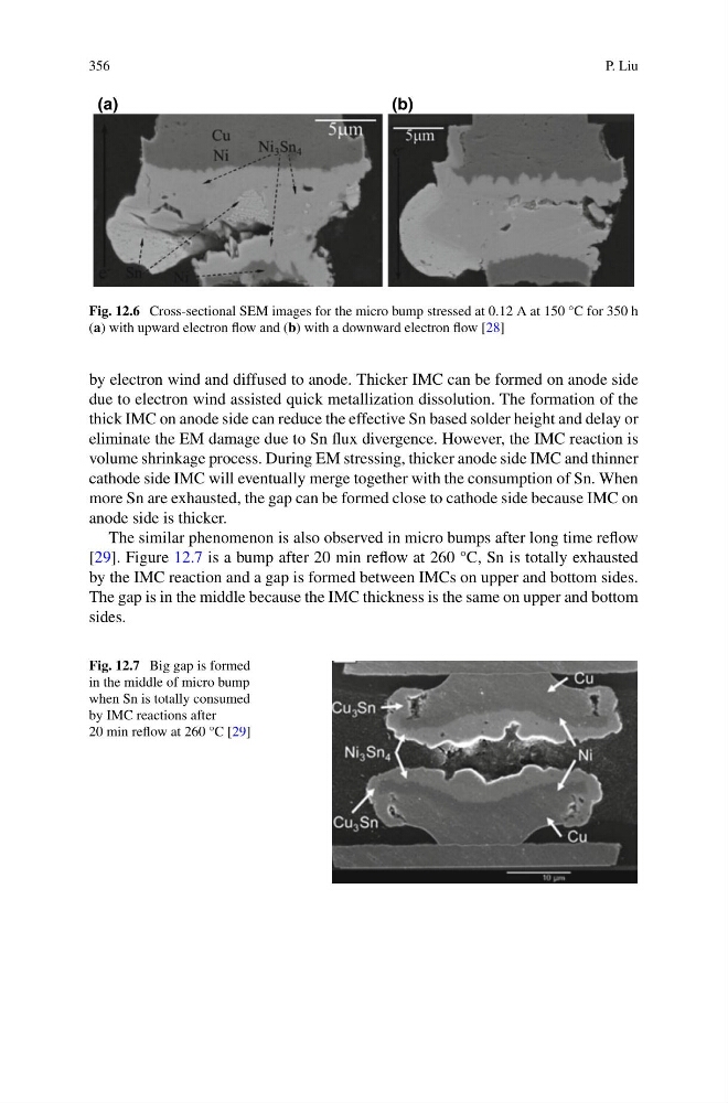
Fig. 12.6 Cross-sectional SEM images for the micro bump stressed at 0.12 A at 150 °C for 350 h
(a) with upward electron flow and (b) with a downward electron flow [28]
by electron wind and diffused to anode. Thicker IMC can be formed on anode side
due to electron wind assisted quick metallization dissolution. The formation of the
thick IMC on anode side can reduce the effective Sn based solder height and delay or
eliminate the EM damage due to Sn flux divergence. However, the IMC reaction is
volume shrinkage process. During EM stressing, thicker anode side IMC and thinner
cathode side IMC will eventually merge together with the consumption of Sn. When
more Sn are exhausted, the gap can be formed close to cathode side because IMC on
anode side is thicker.
The similar phenomenon is also observed in micro bumps after long time reflow
[29]. Figure 12.7 is a bump after 20 min reflow at 260 °C, Sn is totally exhausted
by the IMC reaction and a gap is formed between IMCs on upper and bottom sides.
The gap is in the middle because the IMC thickness is the same on upper and bottom
sides.
Fig. 12.7 Big gap is formed
in the middle of micro bump
when Sn is totally consumed
by IMC reactions after
20 min reflow at 260 °C [29]
P. Liu
(a)
(b)
Fig. 12.6 Cross-sectional SEM images for the micro bump stressed at 0.12 A at 150 °C for 350 h
(a) with upward electron flow and (b) with a downward electron flow [28]
by electron wind and diffused to anode. Thicker IMC can be formed on anode side
due to electron wind assisted quick metallization dissolution. The formation of the
thick IMC on anode side can reduce the effective Sn based solder height and delay or
eliminate the EM damage due to Sn flux divergence. However, the IMC reaction is
volume shrinkage process. During EM stressing, thicker anode side IMC and thinner
cathode side IMC will eventually merge together with the consumption of Sn. When
more Sn are exhausted, the gap can be formed close to cathode side because IMC on
anode side is thicker.
The similar phenomenon is also observed in micro bumps after long time reflow
[29]. Figure 12.7 is a bump after 20 min reflow at 260 °C, Sn is totally exhausted
by the IMC reaction and a gap is formed between IMCs on upper and bottom sides.
The gap is in the middle because the IMC thickness is the same on upper and bottom
sides.
Fig. 12.7 Big gap is formed
in the middle of micro bump
when Sn is totally consumed
by IMC reactions after
20 min reflow at 260 °C [29]