

12 Fundamentals of Electromigration in Interconnects of 3D Packaging
355
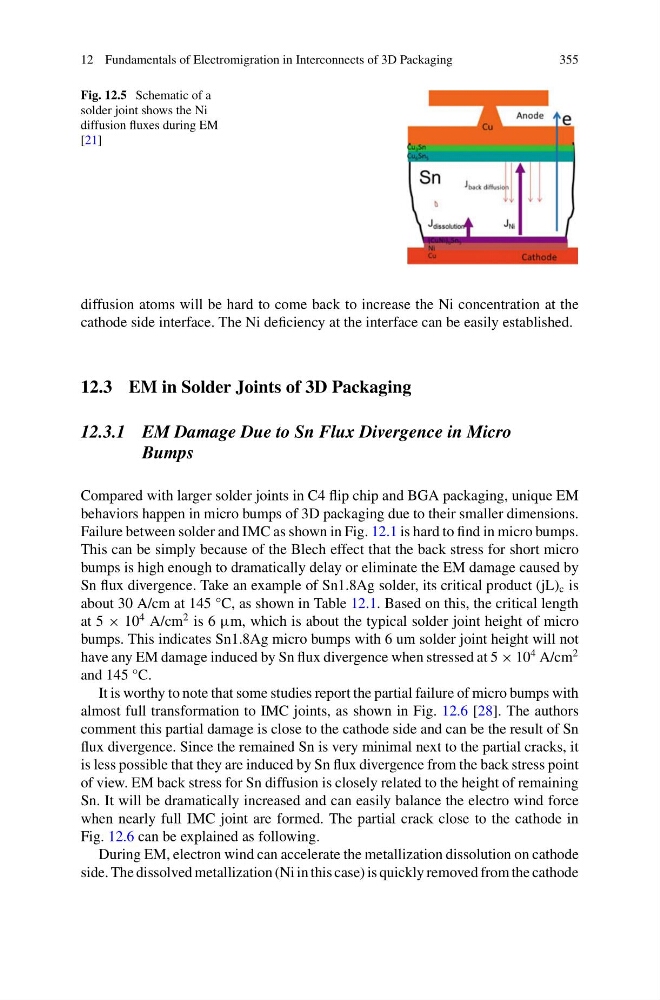
Fig. 12.5 Schematic of a
solder joint shows the Ni
diffusion fluxes during EM
[21]
diffusion atoms will be hard to come back to increase the Ni concentration at the
cathode side interface. The Ni deficiency at the interface can be easily established.
12.3 EM in Solder Joints of 3D Packaging
12.3.1 EM Damage Due to Sn Flux Divergence in Micro
Bumps
Compared with larger solder joints in C4 flip chip and BGA packaging, unique EM
behaviors happen in micro bumps of 3D packaging due to their smaller dimensions.
Failure between solder and IMC as shown in Fig. 12.1 is hard to find in micro bumps.
This can be simply because of the Blech effect that the back stress for short micro
bumps is high enough to dramatically delay or eliminate the EM damage caused by
Sn flux divergence. Take an example of Sn1.8Ag solder, its critical product (jL) c is
about 30 A/cm at 145 °C, as shown in Table 12.1. Based on this, the critical length
at 5 × 10
4 A/cm
2 is 6 μm, which is about the typical solder joint height of micro
bumps. This indicates Sn1.8Ag micro bumps with 6 um solder joint height will not
have any EM damage induced by Sn flux divergence when stressed at 5 × 10
4 A/cm
2
and 145 °C.
It is worthy to note that some studies report the partial failure of micro bumps with
almost full transformation to IMC joints, as shown in Fig. 12.6 [28]. The authors
comment this partial damage is close to the cathode side and can be the result of Sn
flux divergence. Since the remained Sn is very minimal next to the partial cracks, it
is less possible that they are induced by Sn flux divergence from the back stress point
of view. EM back stress for Sn diffusion is closely related to the height of remaining
Sn. It will be dramatically increased and can easily balance the electro wind force
when nearly full IMC joint are formed. The partial crack close to the cathode in
Fig. 12.6 can be explained as following.
During EM, electron wind can accelerate the metallization dissolution on cathode
side. The dissolved metallization (Ni in this case) is quickly removed from the cathode
355
Fig. 12.5 Schematic of a
solder joint shows the Ni
diffusion fluxes during EM
[21]
diffusion atoms will be hard to come back to increase the Ni concentration at the
cathode side interface. The Ni deficiency at the interface can be easily established.
12.3 EM in Solder Joints of 3D Packaging
12.3.1 EM Damage Due to Sn Flux Divergence in Micro
Bumps
Compared with larger solder joints in C4 flip chip and BGA packaging, unique EM
behaviors happen in micro bumps of 3D packaging due to their smaller dimensions.
Failure between solder and IMC as shown in Fig. 12.1 is hard to find in micro bumps.
This can be simply because of the Blech effect that the back stress for short micro
bumps is high enough to dramatically delay or eliminate the EM damage caused by
Sn flux divergence. Take an example of Sn1.8Ag solder, its critical product (jL) c is
about 30 A/cm at 145 °C, as shown in Table 12.1. Based on this, the critical length
at 5 × 10
4 A/cm
2 is 6 μm, which is about the typical solder joint height of micro
bumps. This indicates Sn1.8Ag micro bumps with 6 um solder joint height will not
have any EM damage induced by Sn flux divergence when stressed at 5 × 10
4 A/cm
2
and 145 °C.
It is worthy to note that some studies report the partial failure of micro bumps with
almost full transformation to IMC joints, as shown in Fig. 12.6 [28]. The authors
comment this partial damage is close to the cathode side and can be the result of Sn
flux divergence. Since the remained Sn is very minimal next to the partial cracks, it
is less possible that they are induced by Sn flux divergence from the back stress point
of view. EM back stress for Sn diffusion is closely related to the height of remaining
Sn. It will be dramatically increased and can easily balance the electro wind force
when nearly full IMC joint are formed. The partial crack close to the cathode in
Fig. 12.6 can be explained as following.
During EM, electron wind can accelerate the metallization dissolution on cathode
side. The dissolved metallization (Ni in this case) is quickly removed from the cathode