

358
P. Liu
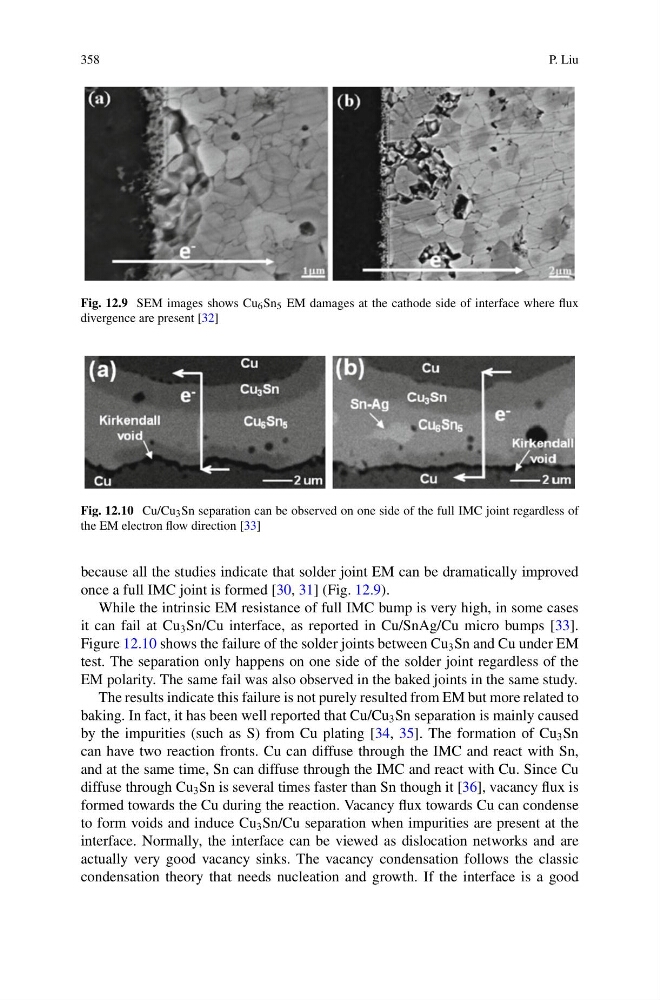
Fig. 12.9 SEM images shows Cu 6 Sn 5 EM damages at the cathode side of interface where flux
divergence are present [32]
Fig. 12.10 Cu/Cu 3 Sn separation can be observed on one side of the full IMC joint regardless of
the EM electron flow direction [33]
because all the studies indicate that solder joint EM can be dramatically improved
once a full IMC joint is formed [30, 31] (Fig. 12.9).
While the intrinsic EM resistance of full IMC bump is very high, in some cases
it can fail at Cu 3 Sn/Cu interface, as reported in Cu/SnAg/Cu micro bumps [33].
Figure 12.10 shows the failure of the solder joints between Cu 3 Sn and Cu under EM
test. The separation only happens on one side of the solder joint regardless of the
EM polarity. The same fail was also observed in the baked joints in the same study.
The results indicate this failure is not purely resulted from EM but more related to
baking. In fact, it has been well reported that Cu/Cu 3 Sn separation is mainly caused
by the impurities (such as S) from Cu plating [34, 35]. The formation of Cu 3 Sn
can have two reaction fronts. Cu can diffuse through the IMC and react with Sn,
and at the same time, Sn can diffuse through the IMC and react with Cu. Since Cu
diffuse through Cu 3 Sn is several times faster than Sn though it [36], vacancy flux is
formed towards the Cu during the reaction. Vacancy flux towards Cu can condense
to form voids and induce Cu 3 Sn/Cu separation when impurities are present at the
interface. Normally, the interface can be viewed as dislocation networks and are
actually very good vacancy sinks. The vacancy condensation follows the classic
condensation theory that needs nucleation and growth. If the interface is a good
P. Liu
Fig. 12.9 SEM images shows Cu 6 Sn 5 EM damages at the cathode side of interface where flux
divergence are present [32]
Fig. 12.10 Cu/Cu 3 Sn separation can be observed on one side of the full IMC joint regardless of
the EM electron flow direction [33]
because all the studies indicate that solder joint EM can be dramatically improved
once a full IMC joint is formed [30, 31] (Fig. 12.9).
While the intrinsic EM resistance of full IMC bump is very high, in some cases
it can fail at Cu 3 Sn/Cu interface, as reported in Cu/SnAg/Cu micro bumps [33].
Figure 12.10 shows the failure of the solder joints between Cu 3 Sn and Cu under EM
test. The separation only happens on one side of the solder joint regardless of the
EM polarity. The same fail was also observed in the baked joints in the same study.
The results indicate this failure is not purely resulted from EM but more related to
baking. In fact, it has been well reported that Cu/Cu 3 Sn separation is mainly caused
by the impurities (such as S) from Cu plating [34, 35]. The formation of Cu 3 Sn
can have two reaction fronts. Cu can diffuse through the IMC and react with Sn,
and at the same time, Sn can diffuse through the IMC and react with Cu. Since Cu
diffuse through Cu 3 Sn is several times faster than Sn though it [36], vacancy flux is
formed towards the Cu during the reaction. Vacancy flux towards Cu can condense
to form voids and induce Cu 3 Sn/Cu separation when impurities are present at the
interface. Normally, the interface can be viewed as dislocation networks and are
actually very good vacancy sinks. The vacancy condensation follows the classic
condensation theory that needs nucleation and growth. If the interface is a good