

12 Fundamentals of Electromigration in Interconnects of 3D Packaging
351
based on accelerated high temperature testing. More efforts are needed to fundamentally understand the physics of temperature impact on (jL) c so that a more accurate
reliability model can be established for solder joints in 3D packaging.
12.2.2 EM Fail Caused by Metallization Dissolution
EM can accelerate the cathode metallization dissolution and promote the formation of
thicker IMC on anode side. When the cathode metallization is thick enough, the joint
can be eventually transformed to a full IMC joint or a joint with very short Sn height
and the EM resistant of the joint can be high. However, when the cathode metallization
is thin, EM can dissolve the entire metallization layer and induce solder joint open [9,
10]. This is a different failure mode from Sn diffusion induced IMC/solder separation
discussed in Sect. 12.2.1. One interesting phenomenon related to this failure mode
is its sensitivity to Sn grain orientations [9, 10, 19–21]. It has been reported that [20]
the time to dissolve 2 um Ni UBM can vary from 100 h (when Sn c-axis is in parallel
to electron flow direction) to 1800 h (when c-axis is perpendicular to electron flow)
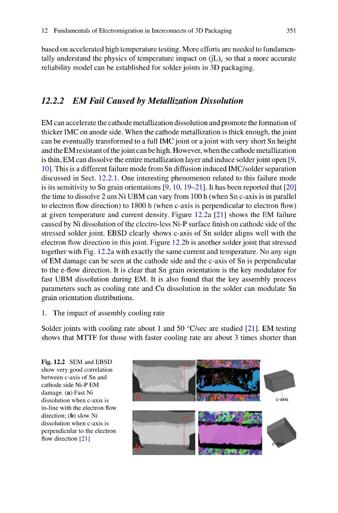
at given temperature and current density. Figure 12.2a [21] shows the EM failure
caused by Ni dissolution of the electro-less Ni-P surface finish on cathode side of the
stressed solder joint. EBSD clearly shows c-axis of Sn solder aligns well with the
electron flow direction in this joint. Figure 12.2b is another solder joint that stressed
together with Fig. 12.2a with exactly the same current and temperature. No any sign
of EM damage can be seen at the cathode side and the c-axis of Sn is perpendicular
to the e-flow direction. It is clear that Sn grain orientation is the key modulator for
fast UBM dissolution during EM. It is also found that the key assembly process
parameters such as cooling rate and Cu dissolution in the solder can modulate Sn
grain orientation distributions.
1. The impact of assembly cooling rate
Solder joints with cooling rate about 1 and 50 °C/sec are studied [21]. EM testing
shows that MTTF for those with faster cooling rate are about 3 times shorter than
Fig. 12.2 SEM and EBSD
show very good correlation
between c-axis of Sn and
cathode side Ni-P EM
damage. (a) Fast Ni
dissolution when c-axis is
in-line with the electron flow
direction; (b) slow Ni
dissolution when c-axis is
perpendicular to the electron
flow direction [21]
351
based on accelerated high temperature testing. More efforts are needed to fundamentally understand the physics of temperature impact on (jL) c so that a more accurate
reliability model can be established for solder joints in 3D packaging.
12.2.2 EM Fail Caused by Metallization Dissolution
EM can accelerate the cathode metallization dissolution and promote the formation of
thicker IMC on anode side. When the cathode metallization is thick enough, the joint
can be eventually transformed to a full IMC joint or a joint with very short Sn height
and the EM resistant of the joint can be high. However, when the cathode metallization
is thin, EM can dissolve the entire metallization layer and induce solder joint open [9,
10]. This is a different failure mode from Sn diffusion induced IMC/solder separation
discussed in Sect. 12.2.1. One interesting phenomenon related to this failure mode
is its sensitivity to Sn grain orientations [9, 10, 19–21]. It has been reported that [20]
the time to dissolve 2 um Ni UBM can vary from 100 h (when Sn c-axis is in parallel
to electron flow direction) to 1800 h (when c-axis is perpendicular to electron flow)
at given temperature and current density. Figure 12.2a [21] shows the EM failure
caused by Ni dissolution of the electro-less Ni-P surface finish on cathode side of the
stressed solder joint. EBSD clearly shows c-axis of Sn solder aligns well with the
electron flow direction in this joint. Figure 12.2b is another solder joint that stressed
together with Fig. 12.2a with exactly the same current and temperature. No any sign
of EM damage can be seen at the cathode side and the c-axis of Sn is perpendicular
to the e-flow direction. It is clear that Sn grain orientation is the key modulator for
fast UBM dissolution during EM. It is also found that the key assembly process
parameters such as cooling rate and Cu dissolution in the solder can modulate Sn
grain orientation distributions.
1. The impact of assembly cooling rate
Solder joints with cooling rate about 1 and 50 °C/sec are studied [21]. EM testing
shows that MTTF for those with faster cooling rate are about 3 times shorter than
Fig. 12.2 SEM and EBSD
show very good correlation
between c-axis of Sn and
cathode side Ni-P EM
damage. (a) Fast Ni
dissolution when c-axis is
in-line with the electron flow
direction; (b) slow Ni
dissolution when c-axis is
perpendicular to the electron
flow direction [21]