

11 Fundamentals of Solder Alloys in 3D Packaging
337
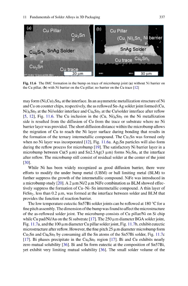
Fig. 11.6 The IMC formation in the bump on trace of microbump joint (a) without Ni barrier on
the Cu pillar, (b) with Ni barrier on the Cu pillar; no barrier on the Cu trace [12]
may form (Ni,Cu) 3 Sn 4 at the interface. In an asymmetric metallization structure of Ni
and Cu on counter chips, respectively, the as reflowed Sn-Ag solder joint formed (Cu,
Ni) 6 Sn 5 at the Ni/solder interface and Cu 6 Sn 5 at the Cu/solder interface after reflow
[5, 12], Fig. 11.6. The Cu inclusion in the (Cu, Ni) 6 Sn 5 on the Ni metallization
side is resulted from the diffusion of Cu from the trace or substrate where no Ni
barrier layer was provided. The short diffusion distance within the microbump allows
the migration of Cu to reach the Ni layer surface during bonding that results in
the formation of the ternary intermetallic compound. The Cu 3 Sn was formed only
when no Ni layer was incorporated [12], Fig. 11.6a. Ag 3 Sn particles will also form
during the reflow process for microbump [19]. The satisfactory Ni barrier layer in a
microbump between Cu(5 µm) and Sn2.5Ag(3 µm) forms Ni 3 Sn 4 at the interface
after reflow. The microbump still consist of residual solder at the center of the joint
[30].
While Ni has been widely recognized as good diffusion barrier, there were
efforts to modify the under bump metal (UBM) or ball limiting metal (BLM) to
further suppress the growth of the intermetallic compound. NiFe was introduced in
a microbump study [20]. A 2 µm Ni/2 µm NiFe combination as BLM showed effectively suppress the formation of Cu–Ni–Sn intermetallic compound. A thin layer of
FeSn 2 , less than 0.2 µm, was formed at the interface between solder and BLM that
provides the function of reaction barrier.
The low temperature eutectic Sn57Bi solder joints can be reflowed at 180 °C for a
fine pitch assembly. The dimension of the bump was found to affect the microstructure
of the as-reflowed solder joint. The microbump consists of Cu pillar/Ni on Si chip
while Cu pad/Ni/Au on the Si substrate [17]. The 250 µm diameter BGA solder joint,
Fig. 11.7a, and the 100 µm diameter Cu pillar solder joint, Fig. 11.7b, exhibit eutectic
microstructure after reflow. However, the fine pitch 25 µm diameter microbump form
Cu 3 Sn and Cu 6 Sn 5 by consuming all the Sn atoms of the Sn57Bi solder, Fig. 11.7c
[17]. Bi phases precipitate in the Cu 6 Sn 5 region [17]. Bi and Cu exhibits nearly
zero mutual solubility [36]. Bi and Sn form eutectic at the composition of Sn57Bi,
yet exhibit very limiting mutual solubility [36]. The small solder volume of the
337
Fig. 11.6 The IMC formation in the bump on trace of microbump joint (a) without Ni barrier on
the Cu pillar, (b) with Ni barrier on the Cu pillar; no barrier on the Cu trace [12]
may form (Ni,Cu) 3 Sn 4 at the interface. In an asymmetric metallization structure of Ni
and Cu on counter chips, respectively, the as reflowed Sn-Ag solder joint formed (Cu,
Ni) 6 Sn 5 at the Ni/solder interface and Cu 6 Sn 5 at the Cu/solder interface after reflow
[5, 12], Fig. 11.6. The Cu inclusion in the (Cu, Ni) 6 Sn 5 on the Ni metallization
side is resulted from the diffusion of Cu from the trace or substrate where no Ni
barrier layer was provided. The short diffusion distance within the microbump allows
the migration of Cu to reach the Ni layer surface during bonding that results in
the formation of the ternary intermetallic compound. The Cu 3 Sn was formed only
when no Ni layer was incorporated [12], Fig. 11.6a. Ag 3 Sn particles will also form
during the reflow process for microbump [19]. The satisfactory Ni barrier layer in a
microbump between Cu(5 µm) and Sn2.5Ag(3 µm) forms Ni 3 Sn 4 at the interface
after reflow. The microbump still consist of residual solder at the center of the joint
[30].
While Ni has been widely recognized as good diffusion barrier, there were
efforts to modify the under bump metal (UBM) or ball limiting metal (BLM) to
further suppress the growth of the intermetallic compound. NiFe was introduced in
a microbump study [20]. A 2 µm Ni/2 µm NiFe combination as BLM showed effectively suppress the formation of Cu–Ni–Sn intermetallic compound. A thin layer of
FeSn 2 , less than 0.2 µm, was formed at the interface between solder and BLM that
provides the function of reaction barrier.
The low temperature eutectic Sn57Bi solder joints can be reflowed at 180 °C for a
fine pitch assembly. The dimension of the bump was found to affect the microstructure
of the as-reflowed solder joint. The microbump consists of Cu pillar/Ni on Si chip
while Cu pad/Ni/Au on the Si substrate [17]. The 250 µm diameter BGA solder joint,
Fig. 11.7a, and the 100 µm diameter Cu pillar solder joint, Fig. 11.7b, exhibit eutectic
microstructure after reflow. However, the fine pitch 25 µm diameter microbump form
Cu 3 Sn and Cu 6 Sn 5 by consuming all the Sn atoms of the Sn57Bi solder, Fig. 11.7c
[17]. Bi phases precipitate in the Cu 6 Sn 5 region [17]. Bi and Cu exhibits nearly
zero mutual solubility [36]. Bi and Sn form eutectic at the composition of Sn57Bi,
yet exhibit very limiting mutual solubility [36]. The small solder volume of the