

338
K.-L. Lin
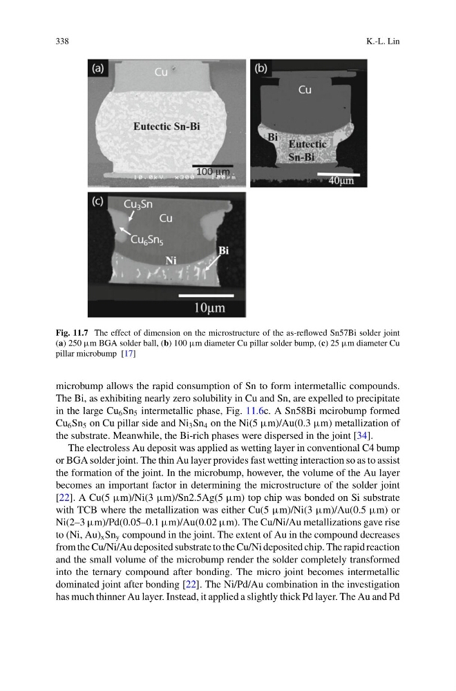
Fig. 11.7 The effect of dimension on the microstructure of the as-reflowed Sn57Bi solder joint
(a) 250 µm BGA solder ball, (b) 100 µm diameter Cu pillar solder bump, (c) 25 µm diameter Cu
pillar microbump [17]
microbump allows the rapid consumption of Sn to form intermetallic compounds.
The Bi, as exhibiting nearly zero solubility in Cu and Sn, are expelled to precipitate
in the large Cu 6 Sn 5 intermetallic phase, Fig. 11.6c. A Sn58Bi mcirobump formed
Cu 6 Sn 5 on Cu pillar side and Ni 3 Sn 4 on the Ni(5 µm)/Au(0.3 µm) metallization of
the substrate. Meanwhile, the Bi-rich phases were dispersed in the joint [34].
The electroless Au deposit was applied as wetting layer in conventional C4 bump
or BGA solder joint. The thin Au layer provides fast wetting interaction so as to assist
the formation of the joint. In the microbump, however, the volume of the Au layer
becomes an important factor in determining the microstructure of the solder joint
[22]. A Cu(5 µm)/Ni(3 µm)/Sn2.5Ag(5 µm) top chip was bonded on Si substrate
with TCB where the metallization was either Cu(5 µm)/Ni(3 µm)/Au(0.5 µm) or
Ni(2–3 µm)/Pd(0.05–0.1 µm)/Au(0.02 µm). The Cu/Ni/Au metallizations gave rise
to (Ni, Au) x Sn y compound in the joint. The extent of Au in the compound decreases
from the Cu/Ni/Au deposited substrate to the Cu/Ni deposited chip. The rapid reaction
and the small volume of the microbump render the solder completely transformed
into the ternary compound after bonding. The micro joint becomes intermetallic
dominated joint after bonding [22]. The Ni/Pd/Au combination in the investigation
has much thinner Au layer. Instead, it applied a slightly thick Pd layer. The Au and Pd
K.-L. Lin
Fig. 11.7 The effect of dimension on the microstructure of the as-reflowed Sn57Bi solder joint
(a) 250 µm BGA solder ball, (b) 100 µm diameter Cu pillar solder bump, (c) 25 µm diameter Cu
pillar microbump [17]
microbump allows the rapid consumption of Sn to form intermetallic compounds.
The Bi, as exhibiting nearly zero solubility in Cu and Sn, are expelled to precipitate
in the large Cu 6 Sn 5 intermetallic phase, Fig. 11.6c. A Sn58Bi mcirobump formed
Cu 6 Sn 5 on Cu pillar side and Ni 3 Sn 4 on the Ni(5 µm)/Au(0.3 µm) metallization of
the substrate. Meanwhile, the Bi-rich phases were dispersed in the joint [34].
The electroless Au deposit was applied as wetting layer in conventional C4 bump
or BGA solder joint. The thin Au layer provides fast wetting interaction so as to assist
the formation of the joint. In the microbump, however, the volume of the Au layer
becomes an important factor in determining the microstructure of the solder joint
[22]. A Cu(5 µm)/Ni(3 µm)/Sn2.5Ag(5 µm) top chip was bonded on Si substrate
with TCB where the metallization was either Cu(5 µm)/Ni(3 µm)/Au(0.5 µm) or
Ni(2–3 µm)/Pd(0.05–0.1 µm)/Au(0.02 µm). The Cu/Ni/Au metallizations gave rise
to (Ni, Au) x Sn y compound in the joint. The extent of Au in the compound decreases
from the Cu/Ni/Au deposited substrate to the Cu/Ni deposited chip. The rapid reaction
and the small volume of the microbump render the solder completely transformed
into the ternary compound after bonding. The micro joint becomes intermetallic
dominated joint after bonding [22]. The Ni/Pd/Au combination in the investigation
has much thinner Au layer. Instead, it applied a slightly thick Pd layer. The Au and Pd