

11 Fundamentals of Solder Alloys in 3D Packaging
335
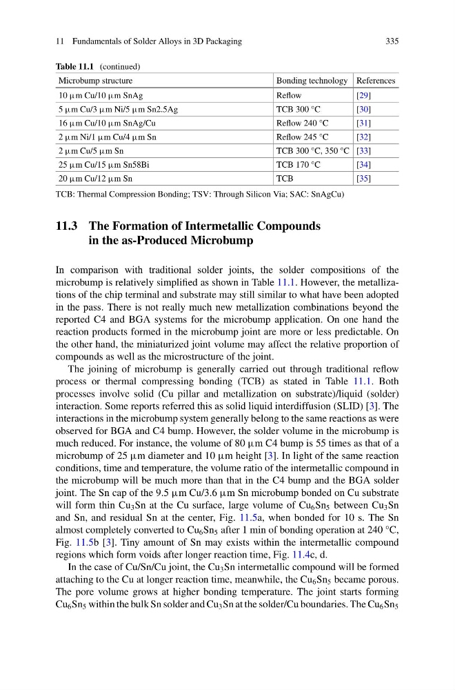
Table 11.1 (continued)
Microbump structure
Bonding technology References
10 µm Cu/10 µm SnAg
Reflow
[29]
5 µm Cu/3 µm Ni/5 µm Sn2.5Ag
TCB 300 °C
[30]
16 µm Cu/10 µm SnAg/Cu
Reflow 240 °C
[31]
2 µm Ni/1 µm Cu/4 µm Sn
Reflow 245 °C
[32]
2 µm Cu/5 µm Sn
TCB 300 °C, 350 °C [33]
25 µm Cu/15 µm Sn58Bi
TCB 170 °C
[34]
20 µm Cu/12 µm Sn
TCB
[35]
TCB: Thermal Compression Bonding; TSV: Through Silicon Via; SAC: SnAgCu)
11.3 The Formation of Intermetallic Compounds
in the as-Produced Microbump
In comparison with traditional solder joints, the solder compositions of the
microbump is relatively simplified as shown in Table 11.1. However, the metallizations of the chip terminal and substrate may still similar to what have been adopted
in the pass. There is not really much new metallization combinations beyond the
reported C4 and BGA systems for the microbump application. On one hand the
reaction products formed in the microbump joint are more or less predictable. On
the other hand, the miniaturized joint volume may affect the relative proportion of
compounds as well as the microstructure of the joint.
The joining of microbump is generally carried out through traditional reflow
process or thermal compressing bonding (TCB) as stated in Table 11.1. Both
processes involve solid (Cu pillar and metallization on substrate)/liquid (solder)
interaction. Some reports referred this as solid liquid interdiffusion (SLID) [3]. The
interactions in the microbump system generally belong to the same reactions as were
observed for BGA and C4 bump. However, the solder volume in the microbump is
much reduced. For instance, the volume of 80 µm C4 bump is 55 times as that of a
microbump of 25 µm diameter and 10 µm height [3]. In light of the same reaction
conditions, time and temperature, the volume ratio of the intermetallic compound in
the microbump will be much more than that in the C4 bump and the BGA solder
joint. The Sn cap of the 9.5 µm Cu/3.6 µm Sn microbump bonded on Cu substrate
will form thin Cu 3 Sn at the Cu surface, large volume of Cu 6 Sn 5 between Cu 3 Sn
and Sn, and residual Sn at the center, Fig. 11.5a, when bonded for 10 s. The Sn
almost completely converted to Cu 6 Sn 5 after 1 min of bonding operation at 240 °C,
Fig. 11.5b [3]. Tiny amount of Sn may exists within the intermetallic compound
regions which form voids after longer reaction time, Fig. 11.4c, d.
In the case of Cu/Sn/Cu joint, the Cu 3 Sn intermetallic compound will be formed
attaching to the Cu at longer reaction time, meanwhile, the Cu 6 Sn 5 became porous.
The pore volume grows at higher bonding temperature. The joint starts forming
Cu 6 Sn 5 within the bulk Sn solder and Cu 3 Sn at the solder/Cu boundaries. The Cu 6 Sn 5
335
Table 11.1 (continued)
Microbump structure
Bonding technology References
10 µm Cu/10 µm SnAg
Reflow
[29]
5 µm Cu/3 µm Ni/5 µm Sn2.5Ag
TCB 300 °C
[30]
16 µm Cu/10 µm SnAg/Cu
Reflow 240 °C
[31]
2 µm Ni/1 µm Cu/4 µm Sn
Reflow 245 °C
[32]
2 µm Cu/5 µm Sn
TCB 300 °C, 350 °C [33]
25 µm Cu/15 µm Sn58Bi
TCB 170 °C
[34]
20 µm Cu/12 µm Sn
TCB
[35]
TCB: Thermal Compression Bonding; TSV: Through Silicon Via; SAC: SnAgCu)
11.3 The Formation of Intermetallic Compounds
in the as-Produced Microbump
In comparison with traditional solder joints, the solder compositions of the
microbump is relatively simplified as shown in Table 11.1. However, the metallizations of the chip terminal and substrate may still similar to what have been adopted
in the pass. There is not really much new metallization combinations beyond the
reported C4 and BGA systems for the microbump application. On one hand the
reaction products formed in the microbump joint are more or less predictable. On
the other hand, the miniaturized joint volume may affect the relative proportion of
compounds as well as the microstructure of the joint.
The joining of microbump is generally carried out through traditional reflow
process or thermal compressing bonding (TCB) as stated in Table 11.1. Both
processes involve solid (Cu pillar and metallization on substrate)/liquid (solder)
interaction. Some reports referred this as solid liquid interdiffusion (SLID) [3]. The
interactions in the microbump system generally belong to the same reactions as were
observed for BGA and C4 bump. However, the solder volume in the microbump is
much reduced. For instance, the volume of 80 µm C4 bump is 55 times as that of a
microbump of 25 µm diameter and 10 µm height [3]. In light of the same reaction
conditions, time and temperature, the volume ratio of the intermetallic compound in
the microbump will be much more than that in the C4 bump and the BGA solder
joint. The Sn cap of the 9.5 µm Cu/3.6 µm Sn microbump bonded on Cu substrate
will form thin Cu 3 Sn at the Cu surface, large volume of Cu 6 Sn 5 between Cu 3 Sn
and Sn, and residual Sn at the center, Fig. 11.5a, when bonded for 10 s. The Sn
almost completely converted to Cu 6 Sn 5 after 1 min of bonding operation at 240 °C,
Fig. 11.5b [3]. Tiny amount of Sn may exists within the intermetallic compound
regions which form voids after longer reaction time, Fig. 11.4c, d.
In the case of Cu/Sn/Cu joint, the Cu 3 Sn intermetallic compound will be formed
attaching to the Cu at longer reaction time, meanwhile, the Cu 6 Sn 5 became porous.
The pore volume grows at higher bonding temperature. The joint starts forming
Cu 6 Sn 5 within the bulk Sn solder and Cu 3 Sn at the solder/Cu boundaries. The Cu 6 Sn 5