

11 Fundamentals of Solder Alloys in 3D Packaging
331
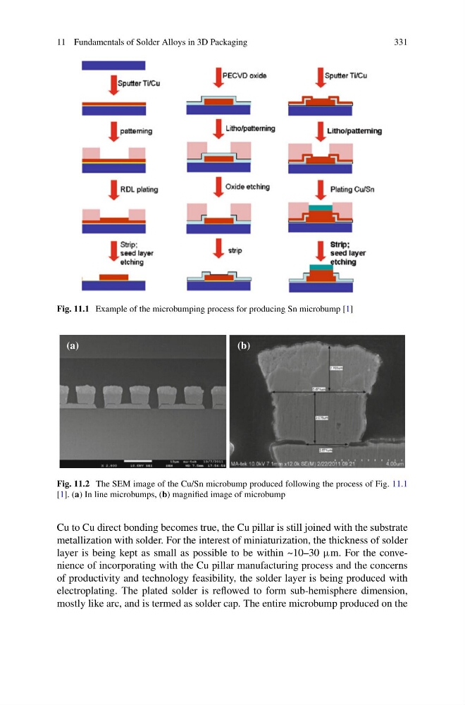
Fig. 11.1 Example of the microbumping process for producing Sn microbump [1]
(a)
(b)
Fig. 11.2 The SEM image of the Cu/Sn microbump produced following the process of Fig. 11.1
[1]. (a) In line microbumps, (b) magnified image of microbump
Cu to Cu direct bonding becomes true, the Cu pillar is still joined with the substrate
metallization with solder. For the interest of miniaturization, the thickness of solder
layer is being kept as small as possible to be within ~10–30 µm. For the convenience of incorporating with the Cu pillar manufacturing process and the concerns
of productivity and technology feasibility, the solder layer is being produced with
electroplating. The plated solder is reflowed to form sub-hemisphere dimension,
mostly like arc, and is termed as solder cap. The entire microbump produced on the
331
Fig. 11.1 Example of the microbumping process for producing Sn microbump [1]
(a)
(b)
Fig. 11.2 The SEM image of the Cu/Sn microbump produced following the process of Fig. 11.1
[1]. (a) In line microbumps, (b) magnified image of microbump
Cu to Cu direct bonding becomes true, the Cu pillar is still joined with the substrate
metallization with solder. For the interest of miniaturization, the thickness of solder
layer is being kept as small as possible to be within ~10–30 µm. For the convenience of incorporating with the Cu pillar manufacturing process and the concerns
of productivity and technology feasibility, the solder layer is being produced with
electroplating. The plated solder is reflowed to form sub-hemisphere dimension,
mostly like arc, and is termed as solder cap. The entire microbump produced on the