

332
K.-L. Lin
chip is thus consisted of the adhesive/conductive layers (in the thickness range of
hundred nanometers) on top of Al trace, the Cu pillar, and the solder cap.
Microbump can be joined on TSV (through silicon via) Cu, substrate Cu pad,
or Cu trace on substrate. The bump on trace process applied thermal compression
bonding to join the microbump on Cu trace line. The Cu trace line being proposed
may adopt OSP-Cu. The OSP can be removed with plasma treatment or with the
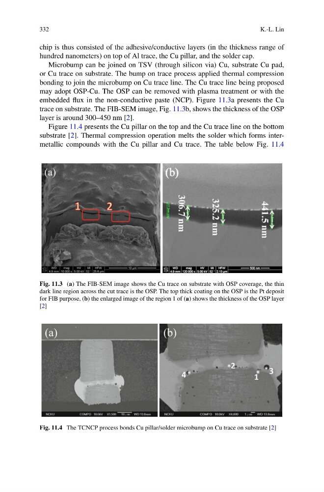
embedded flux in the non-conductive paste (NCP). Figure 11.3a presents the Cu
trace on substrate. The FIB-SEM image, Fig. 11.3b, shows the thickness of the OSP
layer is around 300–450 nm [2].
Figure 11.4 presents the Cu pillar on the top and the Cu trace line on the bottom
substrate [2]. Thermal compression operation melts the solder which forms intermetallic compounds with the Cu pillar and Cu trace. The table below Fig. 11.4
Fig. 11.3 (a) The FIB-SEM image shows the Cu trace on substrate with OSP coverage, the thin
dark line region across the cut trace is the OSP. The top thick coating on the OSP is the Pt deposit
for FIB purpose, (b) the enlarged image of the region 1 of (a) shows the thickness of the OSP layer
[2]
Fig. 11.4 The TCNCP process bonds Cu pillar/solder microbump on Cu trace on substrate [2]
K.-L. Lin
chip is thus consisted of the adhesive/conductive layers (in the thickness range of
hundred nanometers) on top of Al trace, the Cu pillar, and the solder cap.
Microbump can be joined on TSV (through silicon via) Cu, substrate Cu pad,
or Cu trace on substrate. The bump on trace process applied thermal compression
bonding to join the microbump on Cu trace line. The Cu trace line being proposed
may adopt OSP-Cu. The OSP can be removed with plasma treatment or with the
embedded flux in the non-conductive paste (NCP). Figure 11.3a presents the Cu
trace on substrate. The FIB-SEM image, Fig. 11.3b, shows the thickness of the OSP
layer is around 300–450 nm [2].
Figure 11.4 presents the Cu pillar on the top and the Cu trace line on the bottom
substrate [2]. Thermal compression operation melts the solder which forms intermetallic compounds with the Cu pillar and Cu trace. The table below Fig. 11.4
Fig. 11.3 (a) The FIB-SEM image shows the Cu trace on substrate with OSP coverage, the thin
dark line region across the cut trace is the OSP. The top thick coating on the OSP is the Pt deposit
for FIB purpose, (b) the enlarged image of the region 1 of (a) shows the thickness of the OSP layer
[2]
Fig. 11.4 The TCNCP process bonds Cu pillar/solder microbump on Cu trace on substrate [2]