

10 Fundamentals of Bonding Technology and Process Materials …
321
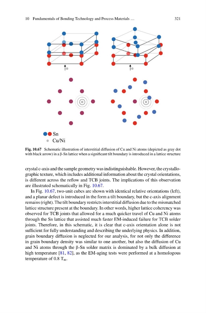
Fig. 10.67 Schematic illustration of interstitial diffusion of Cu and Ni atoms (depicted as gray dot
with black arrow) in a β-Sn lattice when a significant tilt boundary is introduced in a lattice structure
crystal c-axis and the sample geometry was indistinguishable. However, the crystallographic texture, which includes additional information about the crystal orientations,
is different across the reflow and TCB joints. The implications of this observation
are illustrated schematically in Fig. 10.67.
In Fig. 10.67, two-unit cubes are shown with identical relative orientations (left),
and a planar defect is introduced in the form a tilt boundary, but the c-axis alignment
remains (right). The tilt boundary restricts interstitial diffusion due to the mismatched
lattice structure present at the boundary. In other words, higher lattice coherency was
observed for TCB joints that allowed for a much quicker travel of Cu and Ni atoms
through the Sn lattice that assisted much faster EM-induced failure for TCB solder
joints. Therefore, in this schematic, it is clear that c-axis orientation alone is not
sufficient for fully understanding and describing the underlying physics. In addition,
grain boundary diffusion is neglected for our analysis, for not only the difference
in grain boundary density was similar to one another, but also the diffusion of Cu
and Ni atoms through the β-Sn solder matrix is dominated by a bulk diffusion at
high temperature [81, 82], as the EM-aging tests were performed at a homologous
temperature of 0.8 T m .
321
Fig. 10.67 Schematic illustration of interstitial diffusion of Cu and Ni atoms (depicted as gray dot
with black arrow) in a β-Sn lattice when a significant tilt boundary is introduced in a lattice structure
crystal c-axis and the sample geometry was indistinguishable. However, the crystallographic texture, which includes additional information about the crystal orientations,
is different across the reflow and TCB joints. The implications of this observation
are illustrated schematically in Fig. 10.67.
In Fig. 10.67, two-unit cubes are shown with identical relative orientations (left),
and a planar defect is introduced in the form a tilt boundary, but the c-axis alignment
remains (right). The tilt boundary restricts interstitial diffusion due to the mismatched
lattice structure present at the boundary. In other words, higher lattice coherency was
observed for TCB joints that allowed for a much quicker travel of Cu and Ni atoms
through the Sn lattice that assisted much faster EM-induced failure for TCB solder
joints. Therefore, in this schematic, it is clear that c-axis orientation alone is not
sufficient for fully understanding and describing the underlying physics. In addition,
grain boundary diffusion is neglected for our analysis, for not only the difference
in grain boundary density was similar to one another, but also the diffusion of Cu
and Ni atoms through the β-Sn solder matrix is dominated by a bulk diffusion at
high temperature [81, 82], as the EM-aging tests were performed at a homologous
temperature of 0.8 T m .