

322
S. Lee
10.5.4 Conclusion
TCB-processed flip-chip packages have low reliability performance under EM tests
that seemingly limit their potential to be recognized as a highly-reliable bonding
technology. Despite TCB process is in need to fabricate packages with fine-pitch
sized micro-joints for HBM modules and consumer electronics, it has been clarified
from this study that much work is needed in improve its bonding technology.
The EM performance of TCB and the reflow processed solder joints and the
correlations to their microstructure of solder joints has been investigated. The grain
morphology, sizes, orientations and the IMCs were systematically characterized. This
work heightens our understanding on several factors that elucidate for a premature
failure under the EM-aging test. SEM results revealed that the lack of IMC formations
in TCB joints. EBSD and its statistically processed results showed that there is no
difference in misorientation in respective to c-axis orientation; however, relatively
homogenous β-Sn crystallographic textures were observed. Therefore, these factors
could have expedited the failure at the interconnection of the TCB processed package
upon EM-aging test. Further process engineering, such as modifying the process
parameters in the TCB, will be needed to yield the TCB process-3D packages with
improved reliability.
The effect of TCB and reflow bonding on the temperature distribution of solders
was estimated by the finite element analysis (FEA) conducted by Comsol Multiphysics. Unlike the conventional reflow process, TCB process is designed with two
prime sources such as heat and pressure, which derive a coupled engineering analysis
that is complicated and unpredictable. Thus, it is desirable to comprehend a general
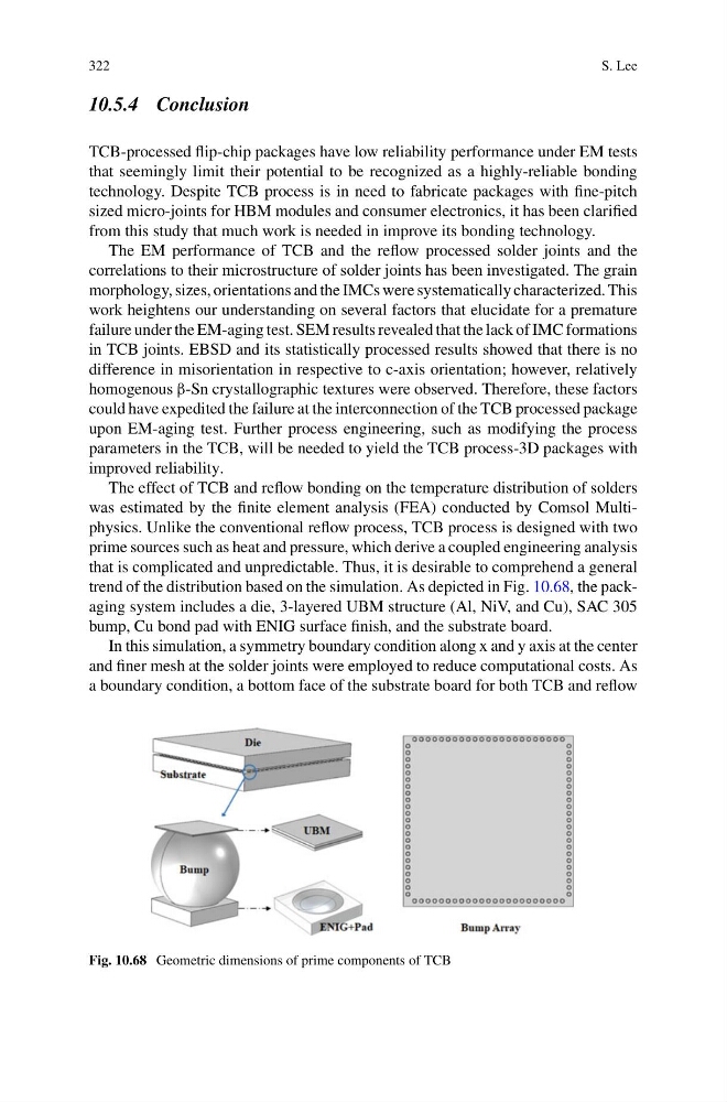
trend of the distribution based on the simulation. As depicted in Fig. 10.68, the packaging system includes a die, 3-layered UBM structure (Al, NiV, and Cu), SAC 305
bump, Cu bond pad with ENIG surface finish, and the substrate board.
In this simulation, a symmetry boundary condition along x and y axis at the center
and finer mesh at the solder joints were employed to reduce computational costs. As
a boundary condition, a bottom face of the substrate board for both TCB and reflow
Fig. 10.68 Geometric dimensions of prime components of TCB
S. Lee
10.5.4 Conclusion
TCB-processed flip-chip packages have low reliability performance under EM tests
that seemingly limit their potential to be recognized as a highly-reliable bonding
technology. Despite TCB process is in need to fabricate packages with fine-pitch
sized micro-joints for HBM modules and consumer electronics, it has been clarified
from this study that much work is needed in improve its bonding technology.
The EM performance of TCB and the reflow processed solder joints and the
correlations to their microstructure of solder joints has been investigated. The grain
morphology, sizes, orientations and the IMCs were systematically characterized. This
work heightens our understanding on several factors that elucidate for a premature
failure under the EM-aging test. SEM results revealed that the lack of IMC formations
in TCB joints. EBSD and its statistically processed results showed that there is no
difference in misorientation in respective to c-axis orientation; however, relatively
homogenous β-Sn crystallographic textures were observed. Therefore, these factors
could have expedited the failure at the interconnection of the TCB processed package
upon EM-aging test. Further process engineering, such as modifying the process
parameters in the TCB, will be needed to yield the TCB process-3D packages with
improved reliability.
The effect of TCB and reflow bonding on the temperature distribution of solders
was estimated by the finite element analysis (FEA) conducted by Comsol Multiphysics. Unlike the conventional reflow process, TCB process is designed with two
prime sources such as heat and pressure, which derive a coupled engineering analysis
that is complicated and unpredictable. Thus, it is desirable to comprehend a general
trend of the distribution based on the simulation. As depicted in Fig. 10.68, the packaging system includes a die, 3-layered UBM structure (Al, NiV, and Cu), SAC 305
bump, Cu bond pad with ENIG surface finish, and the substrate board.
In this simulation, a symmetry boundary condition along x and y axis at the center
and finer mesh at the solder joints were employed to reduce computational costs. As
a boundary condition, a bottom face of the substrate board for both TCB and reflow
Fig. 10.68 Geometric dimensions of prime components of TCB