

10 Fundamentals of Bonding Technology and Process Materials …
313
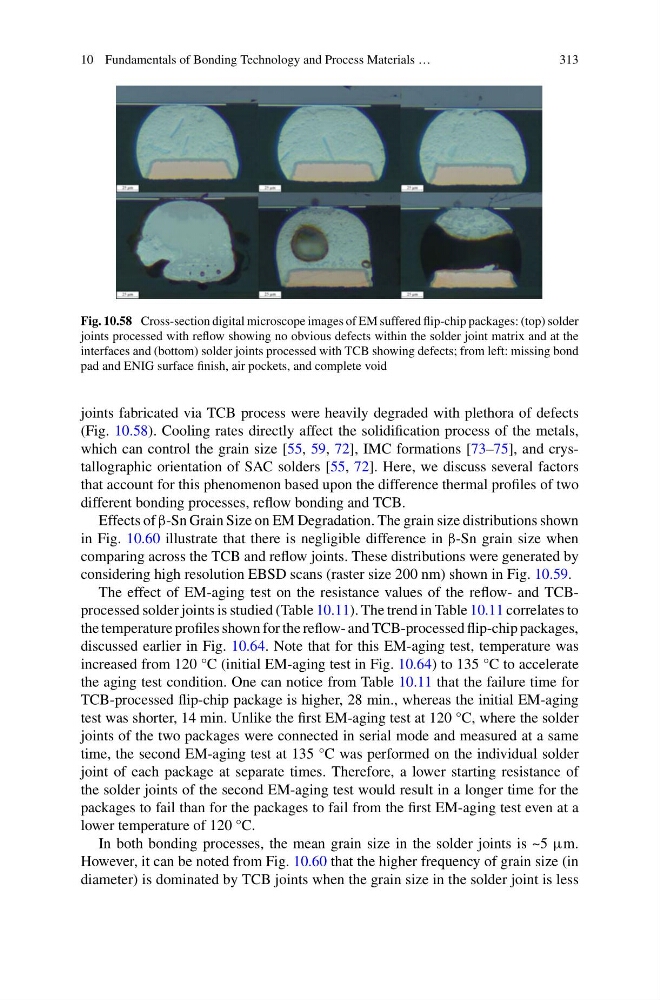
Fig. 10.58 Cross-section digital microscope images of EM suffered flip-chip packages: (top) solder
joints processed with reflow showing no obvious defects within the solder joint matrix and at the
interfaces and (bottom) solder joints processed with TCB showing defects; from left: missing bond
pad and ENIG surface finish, air pockets, and complete void
joints fabricated via TCB process were heavily degraded with plethora of defects
(Fig. 10.58). Cooling rates directly affect the solidification process of the metals,
which can control the grain size [55, 59, 72], IMC formations [73–75], and crystallographic orientation of SAC solders [55, 72]. Here, we discuss several factors
that account for this phenomenon based upon the difference thermal profiles of two
different bonding processes, reflow bonding and TCB.
Effects of β-Sn Grain Size on EM Degradation. The grain size distributions shown
in Fig. 10.60 illustrate that there is negligible difference in β-Sn grain size when
comparing across the TCB and reflow joints. These distributions were generated by
considering high resolution EBSD scans (raster size 200 nm) shown in Fig. 10.59.
The effect of EM-aging test on the resistance values of the reflow- and TCBprocessed solder joints is studied (Table 10.11). The trend in Table 10.11 correlates to
the temperature profiles shown for the reflow- and TCB-processed flip-chip packages,
discussed earlier in Fig. 10.64. Note that for this EM-aging test, temperature was
increased from 120 °C (initial EM-aging test in Fig. 10.64) to 135 °C to accelerate
the aging test condition. One can notice from Table 10.11 that the failure time for
TCB-processed flip-chip package is higher, 28 min., whereas the initial EM-aging
test was shorter, 14 min. Unlike the first EM-aging test at 120 °C, where the solder
joints of the two packages were connected in serial mode and measured at a same
time, the second EM-aging test at 135 °C was performed on the individual solder
joint of each package at separate times. Therefore, a lower starting resistance of
the solder joints of the second EM-aging test would result in a longer time for the
packages to fail than for the packages to fail from the first EM-aging test even at a
lower temperature of 120 °C.
In both bonding processes, the mean grain size in the solder joints is ~5 μm.
However, it can be noted from Fig. 10.60 that the higher frequency of grain size (in
diameter) is dominated by TCB joints when the grain size in the solder joint is less
313
Fig. 10.58 Cross-section digital microscope images of EM suffered flip-chip packages: (top) solder
joints processed with reflow showing no obvious defects within the solder joint matrix and at the
interfaces and (bottom) solder joints processed with TCB showing defects; from left: missing bond
pad and ENIG surface finish, air pockets, and complete void
joints fabricated via TCB process were heavily degraded with plethora of defects
(Fig. 10.58). Cooling rates directly affect the solidification process of the metals,
which can control the grain size [55, 59, 72], IMC formations [73–75], and crystallographic orientation of SAC solders [55, 72]. Here, we discuss several factors
that account for this phenomenon based upon the difference thermal profiles of two
different bonding processes, reflow bonding and TCB.
Effects of β-Sn Grain Size on EM Degradation. The grain size distributions shown
in Fig. 10.60 illustrate that there is negligible difference in β-Sn grain size when
comparing across the TCB and reflow joints. These distributions were generated by
considering high resolution EBSD scans (raster size 200 nm) shown in Fig. 10.59.
The effect of EM-aging test on the resistance values of the reflow- and TCBprocessed solder joints is studied (Table 10.11). The trend in Table 10.11 correlates to
the temperature profiles shown for the reflow- and TCB-processed flip-chip packages,
discussed earlier in Fig. 10.64. Note that for this EM-aging test, temperature was
increased from 120 °C (initial EM-aging test in Fig. 10.64) to 135 °C to accelerate
the aging test condition. One can notice from Table 10.11 that the failure time for
TCB-processed flip-chip package is higher, 28 min., whereas the initial EM-aging
test was shorter, 14 min. Unlike the first EM-aging test at 120 °C, where the solder
joints of the two packages were connected in serial mode and measured at a same
time, the second EM-aging test at 135 °C was performed on the individual solder
joint of each package at separate times. Therefore, a lower starting resistance of
the solder joints of the second EM-aging test would result in a longer time for the
packages to fail than for the packages to fail from the first EM-aging test even at a
lower temperature of 120 °C.
In both bonding processes, the mean grain size in the solder joints is ~5 μm.
However, it can be noted from Fig. 10.60 that the higher frequency of grain size (in
diameter) is dominated by TCB joints when the grain size in the solder joint is less