

314
S. Lee
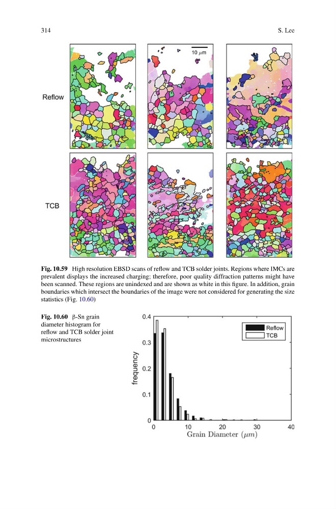
Fig. 10.59 High resolution EBSD scans of reflow and TCB solder joints. Regions where IMCs are
prevalent displays the increased charging; therefore, poor quality diffraction patterns might have
been scanned. These regions are unindexed and are shown as white in this figure. In addition, grain
boundaries which intersect the boundaries of the image were not considered for generating the size
statistics (Fig. 10.60)
Fig. 10.60 β-Sn grain
diameter histogram for
reflow and TCB solder joint
microstructures
S. Lee
Fig. 10.59 High resolution EBSD scans of reflow and TCB solder joints. Regions where IMCs are
prevalent displays the increased charging; therefore, poor quality diffraction patterns might have
been scanned. These regions are unindexed and are shown as white in this figure. In addition, grain
boundaries which intersect the boundaries of the image were not considered for generating the size
statistics (Fig. 10.60)
Fig. 10.60 β-Sn grain
diameter histogram for
reflow and TCB solder joint
microstructures