

10 Fundamentals of Bonding Technology and Process Materials …
311
Fig. 10.55 (left) Bootstrapped mean misorientation density and (right) misorientation density for
reflow and TCB samples. Included are both an angle probability density and the distribution of the
mean c-axis orientation, obtained using bootstrapping
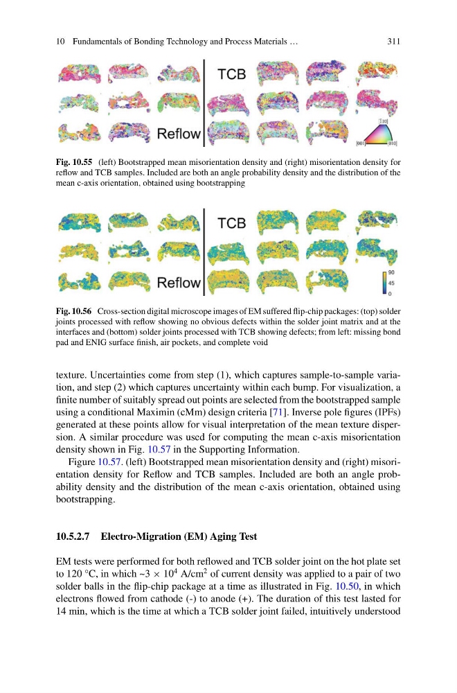
Fig. 10.56 Cross-section digital microscope images of EM suffered flip-chip packages: (top) solder
joints processed with reflow showing no obvious defects within the solder joint matrix and at the
interfaces and (bottom) solder joints processed with TCB showing defects; from left: missing bond
pad and ENIG surface finish, air pockets, and complete void
texture. Uncertainties come from step (1), which captures sample-to-sample variation, and step (2) which captures uncertainty within each bump. For visualization, a
finite number of suitably spread out points are selected from the bootstrapped sample
using a conditional Maximin (cMm) design criteria [71]. Inverse pole figures (IPFs)
generated at these points allow for visual interpretation of the mean texture dispersion. A similar procedure was used for computing the mean c-axis misorientation
density shown in Fig. 10.57 in the Supporting Information.
Figure 10.57. (left) Bootstrapped mean misorientation density and (right) misorientation density for Reflow and TCB samples. Included are both an angle probability density and the distribution of the mean c-axis orientation, obtained using
bootstrapping.
10.5.2.7 Electro-Migration (EM) Aging Test
EM tests were performed for both reflowed and TCB solder joint on the hot plate set
to 120 °C, in which ~3 × 10
4 A/cm
2 of current density was applied to a pair of two
solder balls in the flip-chip package at a time as illustrated in Fig. 10.50, in which
electrons flowed from cathode (-) to anode (+). The duration of this test lasted for
14 min, which is the time at which a TCB solder joint failed, intuitively understood
311
Fig. 10.55 (left) Bootstrapped mean misorientation density and (right) misorientation density for
reflow and TCB samples. Included are both an angle probability density and the distribution of the
mean c-axis orientation, obtained using bootstrapping
Fig. 10.56 Cross-section digital microscope images of EM suffered flip-chip packages: (top) solder
joints processed with reflow showing no obvious defects within the solder joint matrix and at the
interfaces and (bottom) solder joints processed with TCB showing defects; from left: missing bond
pad and ENIG surface finish, air pockets, and complete void
texture. Uncertainties come from step (1), which captures sample-to-sample variation, and step (2) which captures uncertainty within each bump. For visualization, a
finite number of suitably spread out points are selected from the bootstrapped sample
using a conditional Maximin (cMm) design criteria [71]. Inverse pole figures (IPFs)
generated at these points allow for visual interpretation of the mean texture dispersion. A similar procedure was used for computing the mean c-axis misorientation
density shown in Fig. 10.57 in the Supporting Information.
Figure 10.57. (left) Bootstrapped mean misorientation density and (right) misorientation density for Reflow and TCB samples. Included are both an angle probability density and the distribution of the mean c-axis orientation, obtained using
bootstrapping.
10.5.2.7 Electro-Migration (EM) Aging Test
EM tests were performed for both reflowed and TCB solder joint on the hot plate set
to 120 °C, in which ~3 × 10
4 A/cm
2 of current density was applied to a pair of two
solder balls in the flip-chip package at a time as illustrated in Fig. 10.50, in which
electrons flowed from cathode (-) to anode (+). The duration of this test lasted for
14 min, which is the time at which a TCB solder joint failed, intuitively understood