

10 Fundamentals of Bonding Technology and Process Materials …
309
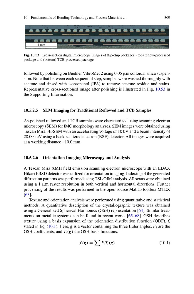
Fig. 10.53 Cross-section digital microscope images of flip-chip packages: (top) reflow-processed
package and (bottom) TCB-processed package
followed by polishing on Buehler VibroMet 2 using 0.05 μm colloidal silica suspension. Note that between each sequential step, samples were washed thoroughly with
acetone and rinsed with isopropanol (IPA) to remove acetone residue and stains.
Representative cross-sectioned image after polishing is illustrated in Fig. 10.53 in
the Supporting Information.
10.5.2.5 SEM Imaging for Traditional Reflowed and TCB Samples
As-polished reflowed and TCB samples were characterized using scanning electron
microscopy (SEM) for IMC morphology analyses. SEM images were obtained using
Tescan Mira FE-SEM with an accelerating voltage of 10 kV and a beam intensity of
20.00 keV using a back-scattered electron (BSE) detector. All images were acquired
at a working distance ~10.0 mm.
10.5.2.6 Orientation Imaging Microscopy and Analysis
A Tescan Mira XMH field emission scanning electron microscope with an EDAX
Hikari EBSD detector was utilized for orientation imaging. Indexing of the generated
diffraction patterns was performed using TSL OIM analysis. All scans were obtained
using a 1 μm raster resolution in both vertical and horizontal directions. Further
processing of the results was performed in the open source Matlab toolbox MTEX
[63].
Texture and orientation analysis were performed using quantitative and statistical
methods. A quantitative description of the crystallographic texture was obtained
using a Generalized Spherical Harmonics (GSH) representation [64]. Similar treatments on metallic systems can be found in recent works [65–68]. GSH describes
texture using a basis expansion of the orientation distribution function (ODF), f,
stated in Eq. (10.1). Here, g is a vector containing the three Euler angles, F i are the
GSH coefficients, and T i (g) the GSH basis functions.
f (g) =
i
F i T i (g)
(10.1)
309
Fig. 10.53 Cross-section digital microscope images of flip-chip packages: (top) reflow-processed
package and (bottom) TCB-processed package
followed by polishing on Buehler VibroMet 2 using 0.05 μm colloidal silica suspension. Note that between each sequential step, samples were washed thoroughly with
acetone and rinsed with isopropanol (IPA) to remove acetone residue and stains.
Representative cross-sectioned image after polishing is illustrated in Fig. 10.53 in
the Supporting Information.
10.5.2.5 SEM Imaging for Traditional Reflowed and TCB Samples
As-polished reflowed and TCB samples were characterized using scanning electron
microscopy (SEM) for IMC morphology analyses. SEM images were obtained using
Tescan Mira FE-SEM with an accelerating voltage of 10 kV and a beam intensity of
20.00 keV using a back-scattered electron (BSE) detector. All images were acquired
at a working distance ~10.0 mm.
10.5.2.6 Orientation Imaging Microscopy and Analysis
A Tescan Mira XMH field emission scanning electron microscope with an EDAX
Hikari EBSD detector was utilized for orientation imaging. Indexing of the generated
diffraction patterns was performed using TSL OIM analysis. All scans were obtained
using a 1 μm raster resolution in both vertical and horizontal directions. Further
processing of the results was performed in the open source Matlab toolbox MTEX
[63].
Texture and orientation analysis were performed using quantitative and statistical
methods. A quantitative description of the crystallographic texture was obtained
using a Generalized Spherical Harmonics (GSH) representation [64]. Similar treatments on metallic systems can be found in recent works [65–68]. GSH describes
texture using a basis expansion of the orientation distribution function (ODF), f,
stated in Eq. (10.1). Here, g is a vector containing the three Euler angles, F i are the
GSH coefficients, and T i (g) the GSH basis functions.
f (g) =
i
F i T i (g)
(10.1)