

10 Fundamentals of Bonding Technology and Process Materials …
291
TCB process. Poor process parameters also can easily generate NCF voids during th
bonding process as other epoxy-based materials do exhibit. Figure 10.34b, c illustrate typical failures that occur in TCB mass production. Indeed, Fig. 10.34b shows
a unique NCF process signature, overflow contamination or compressed fillet, that
have been observed in the NCF building block for TCB technology.
Assuming that epoxy flux is selected for the build block of memory packages or
Application Processor (AP) products, the assembly process requires that the material
to sustain at high temperatures and long time on the bonding stage because a unit will
be bonded one by one to multiple sites on strip form substrate or wafer. Dispensing
epoxy flux on each site right before bonding can be considered to demonstrate feasibility the build block with TCB. However, memory manufactures have not reported
the introduction of epoxy flux in mass production yet.
10.4 Assembly Process Design
10.4.1 Introduction
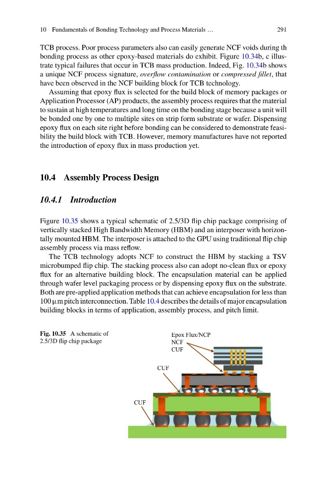
Figure 10.35 shows a typical schematic of 2.5/3D flip chip package comprising of
vertically stacked High Bandwidth Memory (HBM) and an interposer with horizontally mounted HBM. The interposer is attached to the GPU using traditional flip chip
assembly process via mass reflow.
The TCB technology adopts NCF to construct the HBM by stacking a TSV
microbumped flip chip. The stacking process also can adopt no-clean flux or epoxy
flux for an alternative building block. The encapsulation material can be applied
through wafer level packaging process or by dispensing epoxy flux on the substrate.
Both are pre-applied application methods that can achieve encapsulation for less than
100 μm pitch interconnection. Table 10.4 describes the details of major encapsulation
building blocks in terms of application, assembly process, and pitch limit.
Fig. 10.35 A schematic of
2.5/3D flip chip package
CUF
CUF
Epox Flux/NCP
NCF
CUF
291
TCB process. Poor process parameters also can easily generate NCF voids during th
bonding process as other epoxy-based materials do exhibit. Figure 10.34b, c illustrate typical failures that occur in TCB mass production. Indeed, Fig. 10.34b shows
a unique NCF process signature, overflow contamination or compressed fillet, that
have been observed in the NCF building block for TCB technology.
Assuming that epoxy flux is selected for the build block of memory packages or
Application Processor (AP) products, the assembly process requires that the material
to sustain at high temperatures and long time on the bonding stage because a unit will
be bonded one by one to multiple sites on strip form substrate or wafer. Dispensing
epoxy flux on each site right before bonding can be considered to demonstrate feasibility the build block with TCB. However, memory manufactures have not reported
the introduction of epoxy flux in mass production yet.
10.4 Assembly Process Design
10.4.1 Introduction
Figure 10.35 shows a typical schematic of 2.5/3D flip chip package comprising of
vertically stacked High Bandwidth Memory (HBM) and an interposer with horizontally mounted HBM. The interposer is attached to the GPU using traditional flip chip
assembly process via mass reflow.
The TCB technology adopts NCF to construct the HBM by stacking a TSV
microbumped flip chip. The stacking process also can adopt no-clean flux or epoxy
flux for an alternative building block. The encapsulation material can be applied
through wafer level packaging process or by dispensing epoxy flux on the substrate.
Both are pre-applied application methods that can achieve encapsulation for less than
100 μm pitch interconnection. Table 10.4 describes the details of major encapsulation
building blocks in terms of application, assembly process, and pitch limit.
Fig. 10.35 A schematic of
2.5/3D flip chip package
CUF
CUF
Epox Flux/NCP
NCF
CUF