

12
Y. Li and D. Goyal
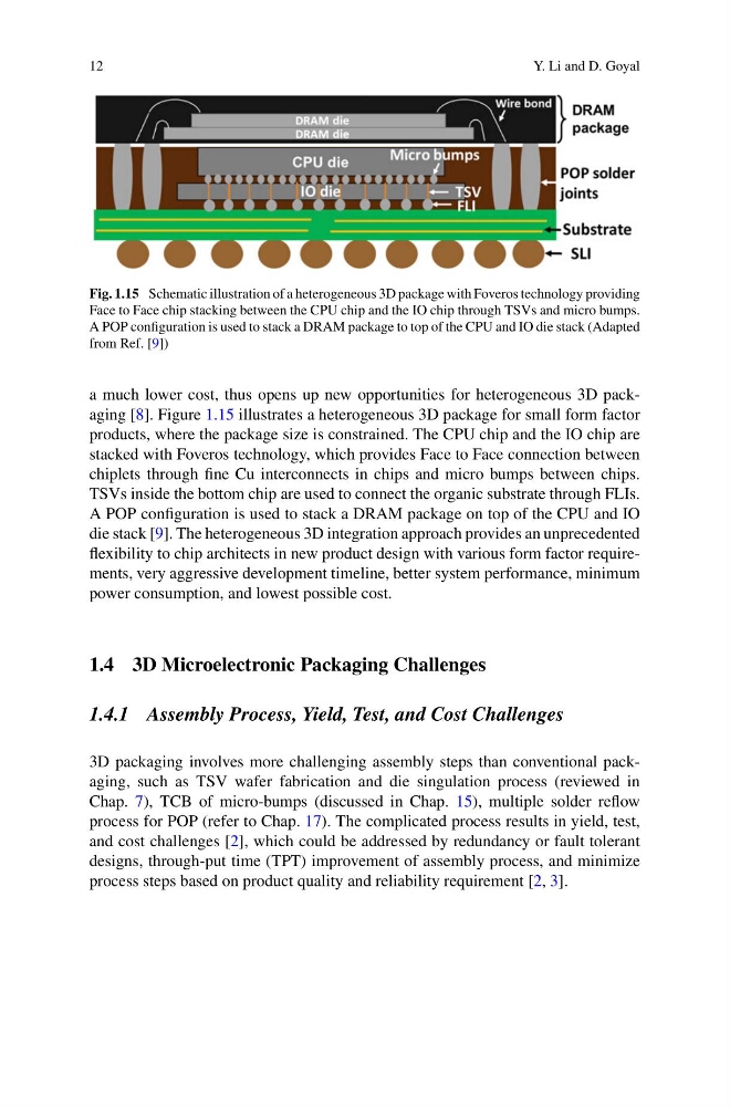
Fig. 1.15 Schematic illustration of a heterogeneous 3D package with Foveros technology providing
Face to Face chip stacking between the CPU chip and the IO chip through TSVs and micro bumps.
A POP configuration is used to stack a DRAM package to top of the CPU and IO die stack (Adapted
from Ref. [9])
a much lower cost, thus opens up new opportunities for heterogeneous 3D packaging [8]. Figure 1.15 illustrates a heterogeneous 3D package for small form factor
products, where the package size is constrained. The CPU chip and the IO chip are
stacked with Foveros technology, which provides Face to Face connection between
chiplets through fine Cu interconnects in chips and micro bumps between chips.
TSVs inside the bottom chip are used to connect the organic substrate through FLIs.
A POP configuration is used to stack a DRAM package on top of the CPU and IO
die stack [9]. The heterogeneous 3D integration approach provides an unprecedented
flexibility to chip architects in new product design with various form factor requirements, very aggressive development timeline, better system performance, minimum
power consumption, and lowest possible cost.
1.4 3D Microelectronic Packaging Challenges
1.4.1 Assembly Process, Yield, Test, and Cost Challenges
3D packaging involves more challenging assembly steps than conventional packaging, such as TSV wafer fabrication and die singulation process (reviewed in
Chap. 7), TCB of micro-bumps (discussed in Chap. 15), multiple solder reflow
process for POP (refer to Chap. 17). The complicated process results in yield, test,
and cost challenges [2], which could be addressed by redundancy or fault tolerant
designs, through-put time (TPT) improvement of assembly process, and minimize
process steps based on product quality and reliability requirement [2, 3].
Y. Li and D. Goyal
Fig. 1.15 Schematic illustration of a heterogeneous 3D package with Foveros technology providing
Face to Face chip stacking between the CPU chip and the IO chip through TSVs and micro bumps.
A POP configuration is used to stack a DRAM package to top of the CPU and IO die stack (Adapted
from Ref. [9])
a much lower cost, thus opens up new opportunities for heterogeneous 3D packaging [8]. Figure 1.15 illustrates a heterogeneous 3D package for small form factor
products, where the package size is constrained. The CPU chip and the IO chip are
stacked with Foveros technology, which provides Face to Face connection between
chiplets through fine Cu interconnects in chips and micro bumps between chips.
TSVs inside the bottom chip are used to connect the organic substrate through FLIs.
A POP configuration is used to stack a DRAM package on top of the CPU and IO
die stack [9]. The heterogeneous 3D integration approach provides an unprecedented
flexibility to chip architects in new product design with various form factor requirements, very aggressive development timeline, better system performance, minimum
power consumption, and lowest possible cost.
1.4 3D Microelectronic Packaging Challenges
1.4.1 Assembly Process, Yield, Test, and Cost Challenges
3D packaging involves more challenging assembly steps than conventional packaging, such as TSV wafer fabrication and die singulation process (reviewed in
Chap. 7), TCB of micro-bumps (discussed in Chap. 15), multiple solder reflow
process for POP (refer to Chap. 17). The complicated process results in yield, test,
and cost challenges [2], which could be addressed by redundancy or fault tolerant
designs, through-put time (TPT) improvement of assembly process, and minimize
process steps based on product quality and reliability requirement [2, 3].