

1 Introduction to 3D Microelectronic Packaging
11
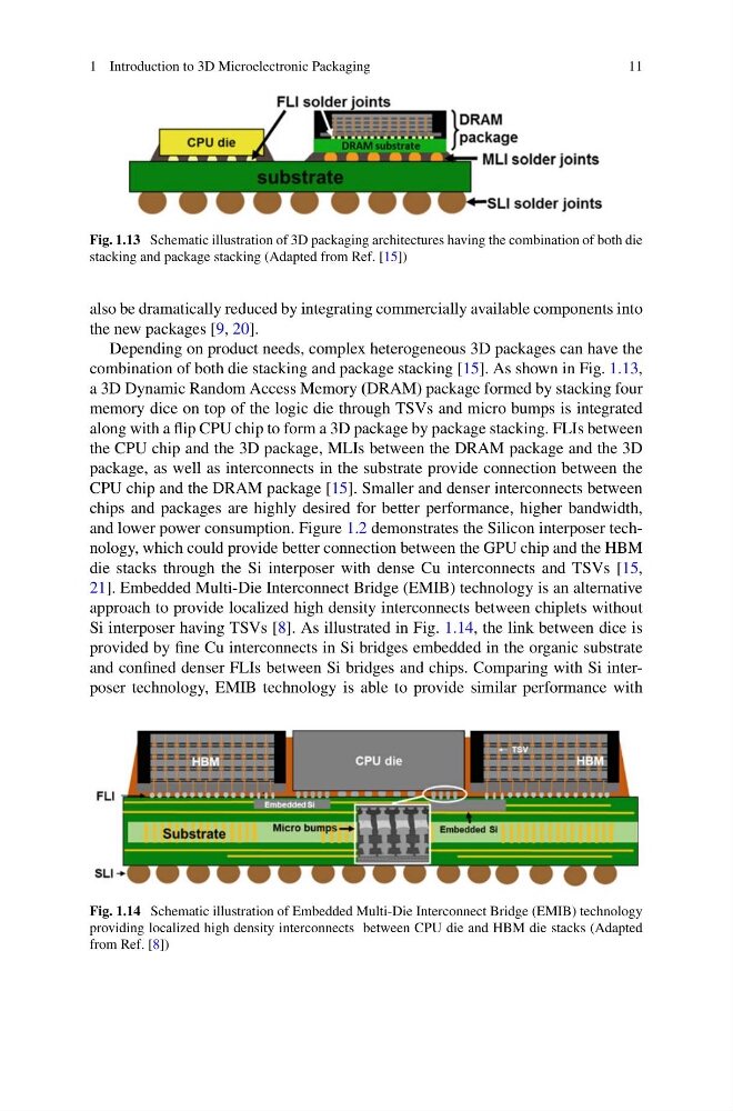
Fig. 1.13 Schematic illustration of 3D packaging architectures having the combination of both die
stacking and package stacking (Adapted from Ref. [15])
also be dramatically reduced by integrating commercially available components into
the new packages [9, 20].
Depending on product needs, complex heterogeneous 3D packages can have the
combination of both die stacking and package stacking [15]. As shown in Fig. 1.13,
a 3D Dynamic Random Access Memory (DRAM) package formed by stacking four
memory dice on top of the logic die through TSVs and micro bumps is integrated
along with a flip CPU chip to form a 3D package by package stacking. FLIs between
the CPU chip and the 3D package, MLIs between the DRAM package and the 3D
package, as well as interconnects in the substrate provide connection between the
CPU chip and the DRAM package [15]. Smaller and denser interconnects between
chips and packages are highly desired for better performance, higher bandwidth,
and lower power consumption. Figure 1.2 demonstrates the Silicon interposer technology, which could provide better connection between the GPU chip and the HBM
die stacks through the Si interposer with dense Cu interconnects and TSVs [15,
21]. Embedded Multi-Die Interconnect Bridge (EMIB) technology is an alternative
approach to provide localized high density interconnects between chiplets without
Si interposer having TSVs [8]. As illustrated in Fig. 1.14, the link between dice is
provided by fine Cu interconnects in Si bridges embedded in the organic substrate
and confined denser FLIs between Si bridges and chips. Comparing with Si interposer technology, EMIB technology is able to provide similar performance with
Fig. 1.14 Schematic illustration of Embedded Multi-Die Interconnect Bridge (EMIB) technology
providing localized high density interconnects between CPU die and HBM die stacks (Adapted
from Ref. [8])
11
Fig. 1.13 Schematic illustration of 3D packaging architectures having the combination of both die
stacking and package stacking (Adapted from Ref. [15])
also be dramatically reduced by integrating commercially available components into
the new packages [9, 20].
Depending on product needs, complex heterogeneous 3D packages can have the
combination of both die stacking and package stacking [15]. As shown in Fig. 1.13,
a 3D Dynamic Random Access Memory (DRAM) package formed by stacking four
memory dice on top of the logic die through TSVs and micro bumps is integrated
along with a flip CPU chip to form a 3D package by package stacking. FLIs between
the CPU chip and the 3D package, MLIs between the DRAM package and the 3D
package, as well as interconnects in the substrate provide connection between the
CPU chip and the DRAM package [15]. Smaller and denser interconnects between
chips and packages are highly desired for better performance, higher bandwidth,
and lower power consumption. Figure 1.2 demonstrates the Silicon interposer technology, which could provide better connection between the GPU chip and the HBM
die stacks through the Si interposer with dense Cu interconnects and TSVs [15,
21]. Embedded Multi-Die Interconnect Bridge (EMIB) technology is an alternative
approach to provide localized high density interconnects between chiplets without
Si interposer having TSVs [8]. As illustrated in Fig. 1.14, the link between dice is
provided by fine Cu interconnects in Si bridges embedded in the organic substrate
and confined denser FLIs between Si bridges and chips. Comparing with Si interposer technology, EMIB technology is able to provide similar performance with
Fig. 1.14 Schematic illustration of Embedded Multi-Die Interconnect Bridge (EMIB) technology
providing localized high density interconnects between CPU die and HBM die stacks (Adapted
from Ref. [8])