

10
Y. Li and D. Goyal
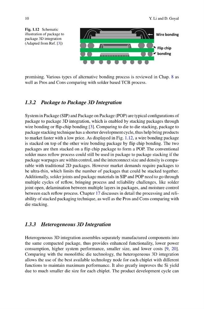
Fig. 1.12 Schematic
illustration of package to
package 3D integration
(Adapted from Ref. [3])
promising. Various types of alternative bonding process is reviewed in Chap. 8 as
well as Pros and Cons comparing with solder based TCB process.
1.3.2 Package to Package 3D Integration
System in Package (SIP) and Package on Package (POP) are typical configurations of
package to package 3D integration, which is enabled by stacking packages through
wire bonding or flip-chip bonding [3]. Comparing to die to die stacking, package to
package stacking technique has a shorter development cycle, thus help bring products
to market faster with a low price. As displayed in Fig. 1.12, a wire bonding package
is stacked on top of the other wire bonding package by flip chip bonding. The two
packages are then stacked on a flip chip package to form a POP. The conventional
solder mass reflow process could still be used in package to package stacking if the
package warpages are within control, and the interconnect size and density is comparable with traditional 2D packages. However market demands require packages to
be ultra-thin, which limits the number of packages that could be stacked together.
Additionally, solder joints and package materials in SIP and POP need to go through
multiple cycles of reflow, bringing process and reliability challenges, like solder
joint open, delamination between multiple layers in packages, and moisture control
between each reflow process. Chapter 17 discusses in detail the processing and reliability of stacked packaging technique, as well as the Pros and Cons comparing with
die stacking.
1.3.3 Heterogeneous 3D Integration
Heterogeneous 3D integration assembles separately manufactured components into
the same compacted package, thus provides enhanced functionality, lower power
consumption, higher system performance, smaller size, and lower costs [9, 20].
Comparing with the monolithic die technology, the heterogeneous 3D integration
allows the use of the best available technology node for each chiplet with different
functions to maintain maximum performance. It also greatly improves the Si yield
due to much smaller die size for each chiplet. The product development cycle can
Y. Li and D. Goyal
Fig. 1.12 Schematic
illustration of package to
package 3D integration
(Adapted from Ref. [3])
promising. Various types of alternative bonding process is reviewed in Chap. 8 as
well as Pros and Cons comparing with solder based TCB process.
1.3.2 Package to Package 3D Integration
System in Package (SIP) and Package on Package (POP) are typical configurations of
package to package 3D integration, which is enabled by stacking packages through
wire bonding or flip-chip bonding [3]. Comparing to die to die stacking, package to
package stacking technique has a shorter development cycle, thus help bring products
to market faster with a low price. As displayed in Fig. 1.12, a wire bonding package
is stacked on top of the other wire bonding package by flip chip bonding. The two
packages are then stacked on a flip chip package to form a POP. The conventional
solder mass reflow process could still be used in package to package stacking if the
package warpages are within control, and the interconnect size and density is comparable with traditional 2D packages. However market demands require packages to
be ultra-thin, which limits the number of packages that could be stacked together.
Additionally, solder joints and package materials in SIP and POP need to go through
multiple cycles of reflow, bringing process and reliability challenges, like solder
joint open, delamination between multiple layers in packages, and moisture control
between each reflow process. Chapter 17 discusses in detail the processing and reliability of stacked packaging technique, as well as the Pros and Cons comparing with
die stacking.
1.3.3 Heterogeneous 3D Integration
Heterogeneous 3D integration assembles separately manufactured components into
the same compacted package, thus provides enhanced functionality, lower power
consumption, higher system performance, smaller size, and lower costs [9, 20].
Comparing with the monolithic die technology, the heterogeneous 3D integration
allows the use of the best available technology node for each chiplet with different
functions to maintain maximum performance. It also greatly improves the Si yield
due to much smaller die size for each chiplet. The product development cycle can